
Semelab plc.
Telephone +44(0)1455 556565. Fax +44(0)1455 552612.
E-mail:
sales@semelab.co.uk
Website:
http://www.semelab.co.uk
Document Number 3346
Issue 1
BDS18
BDS18SMD
BDS18SMD05
BDS19
BDS19SMD
BDS19SMD05
Semelab Plc reserves the right to change test conditions, parameter limits and package dimensions without notice. Information furnished by Semelab is believed
to be both accurate and reliable at the time of going to press. However Semelab assumes no responsibility for any errors or omissions discovered in its use.
Semelab encourages customers to verify that datasheets are current before placing orders.
Semelab plc.
Telephone +44(0)1455 556565. Fax +44(0)1455 552612.
E-mail:
sales@semelab.co.uk
Website:
http://www.semelab.co.uk
BDS18
BDS19
V
CBO
Collector - Base voltage (I
E
= 0)
V
CEO
Collector - Emitter voltage (I
B
= 0)
V
EBO
Emitter - Base voltage (I
C
= 0)
I
E
, I
C
Emitter , Collector current
I
B
Base current
P
tot
Total power dissipation at T
case
75∞C
T
stg
Storage Temperature
T
j
Junction Temperature
≠120V
≠150V
≠120V
≠150V
≠5V
≠8A
≠2A
50W
≠65 TO 200∞C
200∞C
MECHANICAL DATA
Dimensions in mm
SILICON PNP
EPITAXIAL BASE IN
TO220 METAL AND
SMD CERAMIC SURFACE
MOUNT PACKAGES
FEATURES
∑ HERMETIC METAL OR CERAMIC
PACKAGES
∑ HIGH RELIABILITY
∑ MILITARY AND SPACE OPTIONS
∑ SCREENING TO CECC LEVELS
∑ FULLY ISOLATED (METAL VERSION)
APPLICATIONS
∑ POWER LINEAR AND SWITCHING
APPLICATIONS
∑ GENERAL PURPOSE POWER
ABSOLUTE MAXIMUM RATINGS
(T
case
=25∞C unless otherwise stated)
16.
5
13.
5
10.
6
13.
70
2 . 5 4
B S C
1 0. 6
3 . 6
D ia .
0 . 8
4 . 6
1 . 0
2. 70
B S C
1 2 3
3 . 6 0 ( 0 . 1 4 2 )
M a x .
3 . 7 0 ( 0 . 1 4 6 )
3 . 4 1 ( 0 . 1 3 4 )
3 . 7 0 ( 0 . 1 4 6 )
3 . 4 1 ( 0 . 1 3 4 )
0 . 8 9
( 0 . 0 3 5 )
m i n .
4.
14
(
0.
163)
3.
84
(
0.
151)
10.
69
(
0
.
4
21)
10.
39
(
0
.
4
09)
9 . 6 7 ( 0 . 3 8 1 )
9 . 3 8 ( 0 . 3 6 9 )
1 1 . 5 8 ( 0 . 4 5 6 )
1 1 . 2 8 ( 0 . 4 4 4 )
16.
02
(
0
.
6
31)
15.
73
(
0
.
6
19)
0 . 5 0 ( 0 . 0 2 0 )
0 . 2 6 ( 0 . 0 1 0 )
0.
76
(
0
.
030) mi
n
.
1
3
2
SMD1 (TO276AB) Ceramic Surface Mount Package
Pad 1 ≠ Base Pad 2 ≠ Collector Pad 3 ≠ Emitter
SMD05 (TO276AA) Ceramic Surface Mount Package
Pad 1 ≠ Base Pad 2 ≠ Collector Pad 3 ≠ Emitter
Semelab plc.
Telephone +44(0)1455 556565. Fax +44(0)1455 552612.
E-mail:
sales@semelab.co.uk
Website:
http://www.semelab.co.uk
!
0 . 1 2 7 ( 0 . 0 0 5 )
2 . 4 1 ( 0 . 0 9 5 )
( 0 . 0 3 0 )
m i n .
3
.0
5
(
0
.1
2
0
)
5
.
7
2
(
.2
2
5
)
0 . 1 2 7 ( 0 . 0 0 5 )
( 0 . 2 9 6 )
1
0
.
1
6
(
0
.4
0
0
)
0.
76
(
0
.
0
30)
mi
n
.
3 . 1 7 5 ( 0 . 1 2 5 )
M a x .
0 . 5 0 ( 0 . 0 2 0 )
0 . 2 6 ( 0 . 0 1 0 )
7 . 5 4
0 . 7 6
2 . 4 1 ( 0 . 0 9 5 )
0 . 1 2 7 ( 0 . 0 0 5 )
( 0 . 2 8 6 )
7 . 2 6
1 6 P L C S
0 . 5 0 ( 0 . 0 2 0 )
TO220M (TO257AB) Metal Package - Isolated
Pin 1 ≠ Base Pin 2 ≠ Collector Pin 3 ≠ Emitter
Semelab plc.
Telephone +44(0)1455 556565. Fax +44(0)1455 552612.
E-mail:
sales@semelab.co.uk
Website:
http://www.semelab.co.uk
Document Number 3346
Issue 1
BDS18
BDS18SMD
BDS18SMD05
BDS19
BDS19SMD
BDS19SMD05
Semelab Plc reserves the right to change test conditions, parameter limits and package dimensions without notice. Information furnished by Semelab is believed
to be both accurate and reliable at the time of going to press. However Semelab assumes no responsibility for any errors or omissions discovered in its use.
Semelab encourages customers to verify that datasheets are current before placing orders.
Semelab plc.
Telephone +44(0)1455 556565. Fax +44(0)1455 552612.
E-mail:
sales@semelab.co.uk
Website:
http://www.semelab.co.uk
Parameter
Test Conditions
Max.
Unit
R
THj-case
Thermal resistance junction - case
Max. 2.5∞C/W
R
THj-a
Thermal resistance junction - ambient
(TO220 Only)
Max. 62.5∞C/W
Parameter
Test Conditions
Min.
Typ.
Max.
Unit
Collector cut-off current
(I
E
= 0)
Collector cut-off current
(I
B
= 0)
Emitter cut-off current
(I
C
= 0)
Collector - Emitter
sustaining voltage (I
B
= 0)
Collector - Emitter
saturation voltage
Base - Emitter voltage
DC Current gain
Transition frequency
BDS18
V
CB
= ≠120V
BDS19
V
CB
= ≠150V
BDS18
V
CE
= ≠60V
BDS19
V
CE
= ≠75V
V
EB
= ≠5V
BDS18
BDS19
I
C
= ≠0.5A I
B
= ≠0.05A
I
C
= ≠4.0A V
CE
= ≠4A
I
C
= ≠0.5A V
CE
= ≠2V
I
C
= ≠4A
V
CE
= ≠2V
I
C
= ≠0.5A V
CE
= ≠4V
F = 20MHz
≠20
≠20
≠0.1
≠0.1
≠10
≠120
≠150
≠0.4
≠1.5
≠1.0
40
250
15
150
30
µ
A
mA
µ
A
V
V
V
V
MHz
I
CBO
I
CEO
I
EBO
V
CEO(sus)*
V
CE(sat)*
V
BE(on)*
h
FE*
f
T
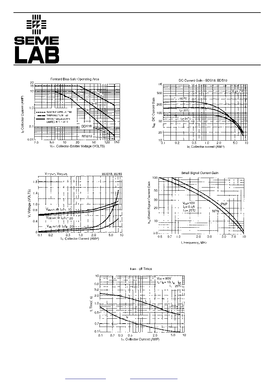
ELECTRICAL CHARACTERISTICS (Tcase = 25∞C unless otherwise stated)
THERMAL DATA
I
C
= ≠100mA
t
on
t
s
t
f
On Time
(t
d
+ t
r
)
Storage Time
Fall Time
I
C
= - 2A V
CC
= ≠80V
I
B1
= 0.2A
I
C
= - 2A V
CC
= ≠80V
I
B1
= ≠I
B2
= 0.2A
0.5
1.5
0.3
µ
s
µ
s
µ
s
SWITCHING CHARACTERISTICS
*Pulsed : Pulse duration = 300
µ
s , duty cycle = 1.5%
Semelab plc.
Telephone +44(0)1455 556565. Fax +44(0)1455 552612.
E-mail:
sales@semelab.co.uk
Website:
http://www.semelab.co.uk
Document Number 3346
Issue 1
BDS18
BDS18SMD
BDS18SMD05
BDS19
BDS19SMD
BDS19SMD05
Semelab Plc reserves the right to change test conditions, parameter limits and package dimensions without notice. Information furnished by Semelab is believed
to be both accurate and reliable at the time of going to press. However Semelab assumes no responsibility for any errors or omissions discovered in its use.
Semelab encourages customers to verify that datasheets are current before placing orders.