BDX63
BDX63A
BDX63B
BDX63C
NPN EPITAXIAL BASE
DARLINGTON POWER
TRANSISTOR
NPN epitaxial base transistors in
monolithic Darlington circuit for
audio output stages and general
amplifier and switching
applications.
PNP complements are:
BDX62, BDX62A, BDX62B, BDX62C.
V
CEO
Collector - emitter voltage (open base)
V
CBO
Collector - base voltage (open emitter)
V
EBO
Emitter - base voltage (open collector)
I
C
Collector current
I
CM
Collector current (peak)
I
B
Base current
P
tot
Total power dissipation at T
case
= 25�C
T
j
Maximum junction temperature
T
stj
Storage junction temperature
R
th j-mb
Thermal resistance, junction to mounting base.
60
80
100
120
V
80
100
120
140
V
5
5
5
5
V
8
A
12
A
150
mA
90
W
200
�C
-65 to 200
�C
1.94
�C / W
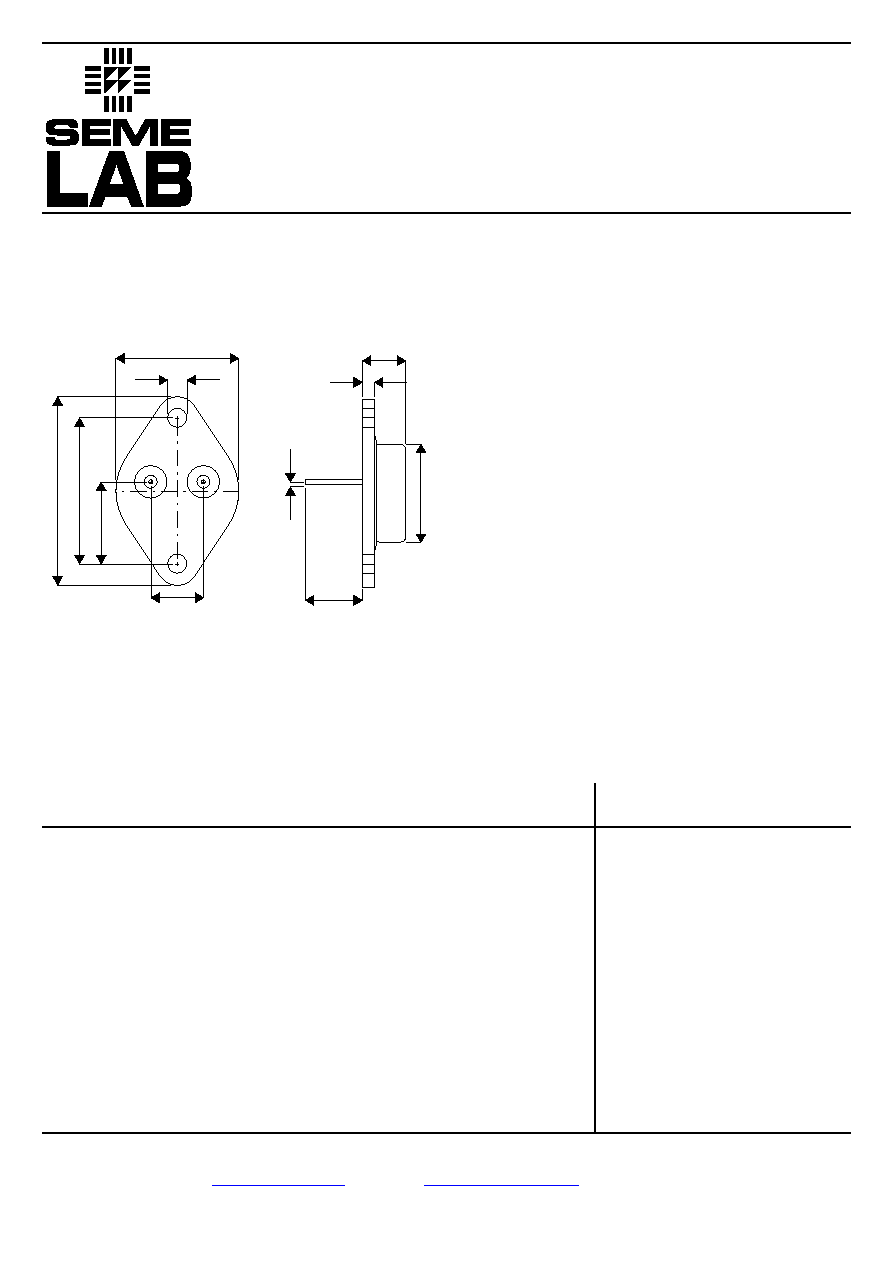
MECHANICAL DATA
Dimensions in mm
ABSOLUTE MAXIMUM RATINGS
(Tcase=25�C unless otherwise stated)
� � � � � � � � � � �
TO3 Package.
Case connected to collector.
BDX BDX BDX BDX
63
63A
63B
63C
B
E
4 . 2
26.6 max.
39.
5 m
a
x
.
30
.
1
16.
9
1 0.9
2. 5
1.
0
12 .8
2
0
.3
m
a
x
.
9.0 max.
Prelim. 7/93
Semelab plc.
Telephone +44(0)1455 556565. Fax +44(0)1455 552612.
E-mail:
sales@semelab.co.uk
Website:
http://www.semelab.co.uk
ELECTRICAL CHARACTERISTICS
(Tj = 25�C, unless otherwise stated)
I
CEO
Collector cut-off current
I
EBO
Emitter cut-off current
h
FE
D.C. current gain (note 1)
V
BE
Base - emitter voltage (note 1)
C
c
Collector capacitance
f
hfe
Cut-off frequency
�
h
fe�
Small signal current gain
V
F
Diode, forward voltage
I
E
= 0, V
CB
= V
CEOmax
I
E
= 0, V
CB
= �V
CBOmax,
T
j
= 200�C
I
B
= 0, V
CE
= �V
CEOmax
I
C
= 0, V
EB
= 5V
I
C
= 0.5A, V
CE
= 3V
I
C
= 3A, V
CE
= 3V
I
C
= 8A, V
CE
= 3V
I
C
= 3A, V
CE
= 3V
I
E
= I
e
= 0, V
CB
= 10V
I
C
= 3A, V
CE
= 3V
�I
Boff
= 0, I
Con
= 4.5 A
t
p
= 1ms, T = 100ms
I
C
= 3A, V
CE
= 3V, f = 1MHz
I
F
= 3A
0.2
2
0.5
5
2500
1000
2600
2.5
100
100
100
1.2
Parameter
Test Conditions
Min.
Typ.
Max.
Unit.
mA
mA
V
pF
kHz
V
Note 1: Measured under pulse conditions , t
p
< 300
ms, d < 2%
2
E
(BR)
Turn-off breakdown energy
with inductive load
h
FE1
/h
FE2
D.C. current gain ratio of
complementary matched pairs
V
CEsat
Collector - emitter saturation
voltage
I
C
= 3A, I
B
= 12mA
V
50
2.5
mJ
I
C
= 3A, V
CE
= 3V
I
CBO
Collector cut-off current
mA
BDX63
BDX63A
BDX63B
BDX63C
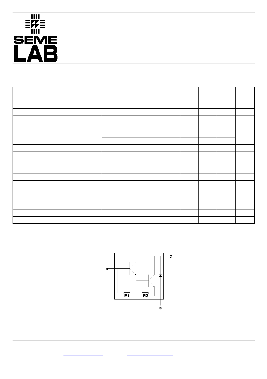
R1 typ. 8K
W
R2 typ. 100
W
Circuit diagram.
Prelim. 7/93
Semelab plc.
Telephone +44(0)1455 556565. Fax +44(0)1455 552612.
E-mail:
sales@semelab.co.uk
Website:
http://www.semelab.co.uk