 | –≠–ª–µ–∫—Ç—Ä–æ–Ω–Ω—ã–π –∫–æ–º–ø–æ–Ω–µ–Ω—Ç: D1221UK | –°–∫–∞—á–∞—Ç—å:  PDF PDF  ZIP ZIP |
D1221UK
Document Number 5316
Issue 1
Semelab plc.
Telephone +44(0)1455 556565. Fax +44(0)1455 552612.
E-mail:
sales@semelab.co.uk
Website:
http://www.semelab.co.uk
Semelab Plc reserves the right to change test conditions, parameter limits and package dimensions without notice. Information furnished by Semelab is believed
to be both accurate and reliable at the time of going to press. However Semelab assumes no responsibility for any errors or omissions discovered in its use.
Semelab encourages customers to verify that datasheets are current before placing orders.
P
D
Power Dissipation
BV
DSS
Drain ≠ Source Breakdown Voltage
BV
GSS
Gate ≠ Source Breakdown Voltage
I
D(sat)
Drain Current
T
stg
Storage Temperature
T
j
Maximum Operating Junction Temperature
50W
40V
±20V
10A
≠65 to 150∞C
200∞C
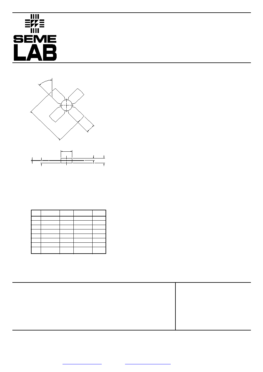
MECHANICAL DATA
4
1
3
2
E
F
A
C
D
G
H
B
GOLD METALLISED
MULTI-PURPOSE SILICON
DMOS RF FET
10W ≠ 12.5V ≠ 175MHz
SINGLE ENDED
FEATURES
∑ SIMPLIFIED AMPLIFIER DESIGN
∑ SUITABLE FOR BROAD BAND APPLICATIONS
∑ LOW C
rss
∑ SIMPLE BIAS CIRCUITS
∑ LOW NOISE
∑ HIGH GAIN ≠ 10 dB MINIMUM
DW
PIN 1
DRAIN
PIN 3
GATE
PIN 2
SOURCE
PIN 4
SOURCE
ABSOLUTE MAXIMUM RATINGS
(T
case
= 25∞C unless otherwise stated)
APPLICATIONS
∑ HF/VHF/UHF COMMUNICATIONS
from 1 MHz to 175 MHz
METAL GATE RF SILICON FET
TetraFET
DIM
mm
Tol.
Inches
Tol.
A
26.16
0.38
1.030
0.015
B
5.72
0.13
0.225
0.005
C
45∞
5∞
45∞
5∞
D
7.11
0.13
0.280
0.005
E
0.13
0.03
0.005
0.001
F
1.52
0.13
0.055
0.005
G
0.43
0.20
0.060
0.008
H
7.67
REF
0.120
REF

D1221UK
Document Number 5316
Issue 1
Semelab plc.
Telephone +44(0)1455 556565. Fax +44(0)1455 552612.
E-mail:
sales@semelab.co.uk
Website:
http://www.semelab.co.uk
Semelab Plc reserves the right to change test conditions, parameter limits and package dimensions without notice. Information furnished by Semelab is believed
to be both accurate and reliable at the time of going to press. However Semelab assumes no responsibility for any errors or omissions discovered in its use.
Semelab encourages customers to verify that datasheets are current before placing orders.
Parameter
Test Conditions
Min.
Typ.
Max.
Unit
V
GS
= 0
I
D
= 100mA
V
DS
= 12.5V
V
GS
= 0
V
GS
= 20V
V
DS
= 0
I
D
= 10mA
V
DS
= V
GS
V
DS
= 10V
I
D
= 1A
P
O
= 10W
V
DS
= 12.5V
I
DQ
= 0.4A
f = 175MHz
V
DS
= 0
V
GS
= ≠5V f = 1MHz
V
DS
= 12.5V V
GS
= 0
f = 1MHz
V
DS
= 12.5V V
GS
= 0
f = 1MHz
V
mA
µ
A
V
S
dB
%
--
pF
pF
pF
ELECTRICAL CHARACTERISTICS
(T
case
= 25∞C unless otherwise stated)
Drain≠Source
BV
DSS
Breakdown Voltage
Zero Gate Voltage
I
DSS
Drain Current
I
GSS
Gate Leakage Current
V
GS(th)
Gate Threshold Voltage*
g
fs
Forward Transconductance*
G
PS
Common Source Power Gain
Drain Efficiency
VSWR
Load Mismatch Tolerance
C
iss
Input Capacitance
C
oss
Output Capacitance
C
rss
Reverse Transfer Capacitance
40
1
1
1
7
0.8
10
50
20:1
60
40
4
HAZARDOUS MATERIAL WARNING
The ceramic portion of the device between leads and metal flange is beryllium oxide. Beryllium oxide dust is highly
toxic and care must be taken during handling and mounting to avoid damage to this area.
THESE DEVICES MUST NEVER BE THROWN AWAY WITH GENERAL INDUSTRIAL OR DOMESTIC WASTE.
R
THj≠case
Thermal Resistance Junction ≠ Case
Max. 3.5∞C / W
THERMAL DATA
* Pulse Test:
Pulse Duration = 300
µ
s , Duty Cycle
2%
D1221UK
Document Number 5316
Issue 1
Semelab plc.
Telephone +44(0)1455 556565. Fax +44(0)1455 552612.
E-mail:
sales@semelab.co.uk
Website:
http://www.semelab.co.uk
Semelab Plc reserves the right to change test conditions, parameter limits and package dimensions without notice. Information furnished by Semelab is believed
to be both accurate and reliable at the time of going to press. However Semelab assumes no responsibility for any errors or omissions discovered in its use.
Semelab encourages customers to verify that datasheets are current before placing orders.
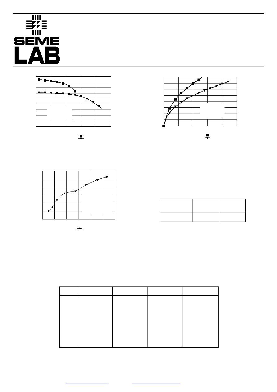
3RXW:
*DLQG%
7XQHGIRUPD[LPXPJDLQDW:
7XQHGIRUPD[LPXPRXWSXWSRZHU
9GV 9
,GT $
I 0+]
3RXW:
(IILFLHQF\
7XQHGIRUPD[LPXPJDLQDW:
7XQHGIRUPD[LPXPRXWSXWSRZHU
9GV 9
,GT $
I 0+]
Figure 1 ≠ Gain vs. Power Output.
Figure 2 ≠ Efficiency vs. Power Output.
3RXW:3(3
,0'
G%F
7XQHGIRUPD[LPXPRXWSXWSRZHU
I 0+]
I 0+]
9GV 9
,GT $
Figure 3 ≠ IMD vs. Power Output.
D1221UK
OPTIMUM SOURCE AND LOAD IMPEDANCE
Frequency
Z
S
Z
L
MHz
175MHz
7.2 + j15 4.1 - j2.5
!Freq
!MHz
mag
ang
mag
ang
mag
ang
mag
ang
50
0.7
-116.5
14.93
97.9
0.036
15.7
0.64
-108.4
100
0.7
-140
7.42
73.6
0.03
2.7
0.65
-132
150
0.75
-150.2
4.56
58.1
0.02
11
0.71
-143.1
200
0.81
-157.2
3.1
46.5
0.016
52.3
0.78
-151.2
250
0.85
-163.1
2.23
37.4
0.026
82.6
0.83
-157.9
300
0.88
-168.1
1.67
30.3
0.04
90.1
0.86
-163.7
350
0.9
-172.6
1.3
24.7
0.055
90.8
0.89
-168.8
400
0.92
-176.6
1.04
20.3
0.071
89.2
0.91
-173.4
450
0.93
179.7
0.85
17.1
0.086
86.8
0.92
-177.5
500
0.94
176.3
0.71
14.9
0.101
84.2
0.93
178.7
550
0.95
173.1
0.6
13.5
0.115
81.5
0.94
175.2
600
0.95
170.
0.52
13
0.13
78.8
0.95
171.
S11
S21
S12
S22
!
V
DS
= 12.5V, I
DQ
= 0.4A
#
MHZ
S MA R 50
Typical S Parameters

D1221UK
Document Number 5316
Issue 1
Semelab plc.
Telephone +44(0)1455 556565. Fax +44(0)1455 552612.
E-mail:
sales@semelab.co.uk
Website:
http://www.semelab.co.uk
Semelab Plc reserves the right to change test conditions, parameter limits and package dimensions without notice. Information furnished by Semelab is believed
to be both accurate and reliable at the time of going to press. However Semelab assumes no responsibility for any errors or omissions discovered in its use.
Semelab encourages customers to verify that datasheets are current before placing orders.
.
.
/
/
Q)
Q)
S)
S)
/
S)
Q)
Q)
X)
/
S)
S)
D1221UK
7
7
*DWH%LDV
7
[PP
FRQWDFWSDG
[PP
FRQWDFWSDG
7
9
$OOPLFURVWULSOLQHV: PP
6XEVWUDWHPP37)(JODVV(U
/WXUQVVZJHQDPHOOHGFRSSHUZLUHPPLG
7PP
7PP
7PP
7PP
/ WXUQVVZJHQDPHOOHGFRSSHUZLUHPPLG
/ WXUQVVZJHQDPHOOHGFRSSHUZLUHPPLG
/WXUQVVZJHQDPHOOHGFRSSHUZLUHRQ6LHPHQV
%$;IHUULWHFRUH
D1221UK 175MHz TEST FIXTURE