 | –≠–ª–µ–∫—Ç—Ä–æ–Ω–Ω—ã–π –∫–æ–º–ø–æ–Ω–µ–Ω—Ç: IP1526J | –°–∫–∞—á–∞—Ç—å:  PDF PDF  ZIP ZIP |

IP1526 SERIES
4/99
Semelab plc.
Telephone +44(0)1455 556565. Fax +44(0)1455 552612.
E-mail:
sales@semelab.co.uk
Website:
http://www.semelab.co.uk
Semelab plc.
Telephone +44(0)1455 556565. Fax +44(0)1455 552612.
E-mail:
sales@semelab.co.uk
Website:
http://www.semelab.co.uk
REGULATING
PULSE WIDTH
MODULATOR
FEATURES
∑ 8 to 35V operation
∑ 5V reference trimmed to ±1%
∑ 1Hz to 400kHz oscillator range
∑ Dual 100mA source/sink outputs
∑ Digital current limiting
∑ Double pulse suppression
∑ Programmable deadtime
∑ Undervoltage lockout
∑ Single Pulse metering
∑ Programmable soft start
∑ Wide current limit common mode range
∑ TTL/CMOS compatible logic ports
∑ Symmetry correction capability
∑ Guaranteed 6 unit synchronisation
+V
IN
Input Voltage
Collector Supply Voltage
Logic Inputs
Analogue Inputs
Source / Sink Load Current
Reference Load Current
Logic Sink Current
P
D
Power Dissipation
T
A
= 25∞C
Derate @ T
A
> 50∞C
P
D
Power Dissipation
T
C
= 25∞C
Derate @ T
C
> 25∞C
T
J
Operating Junction Temperature
T
STG
Storage Temperature Range
T
L
Lead Temperature
(soldering, 10 seconds)
+40V
+40V
≠0.3 to +5.5V
≠0.3 to +V
IN
200mA
Internally Limited
15mA
1W
10mW/∞C
3W
24mW/∞C
See Ordering Information
≠65 to +150∞C
+300∞C
ABSOLUTE MAXIMUM RATINGS
(T
case
= 25∞C unless otherwise stated)
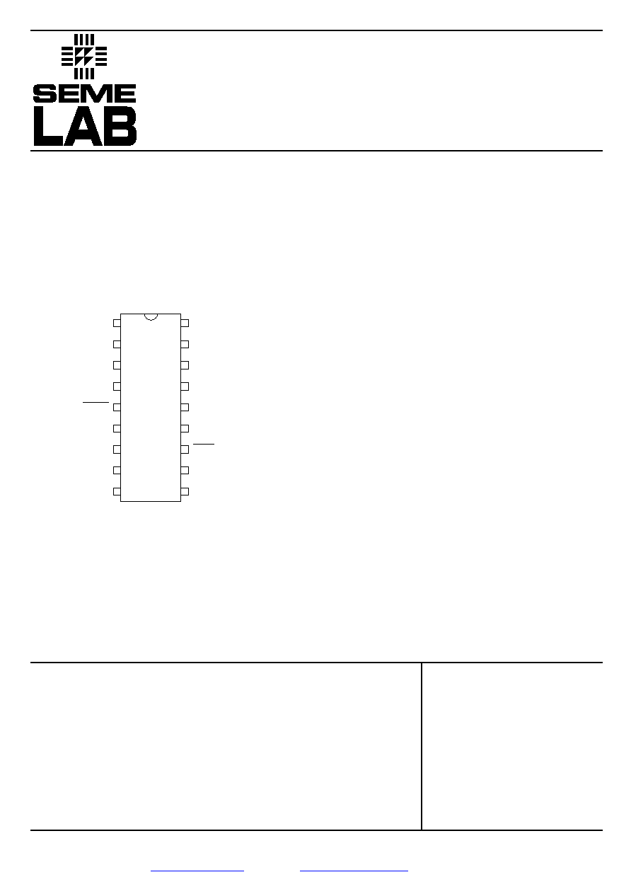
TOP VIEW
J Package ≠ 18 Pin Ceramic DIP
N Package ≠ 18 Pin Plastic DIP
DW Package ≠ 18 Pin Plastic (300) SOIC
8
1
2
3
4
5
6
7
14
13
12
11
10
9
15
16
17
18
V
REF
OUTPUT B
GROUND
OUTPUT A
+ERROR
≠ERROR
COMPENSATION
SOFTSTART
C
RESET
+CURRENT SENSE
≠CURRENT SENSE
SHUTDOWN
C
TIMING
R
TIMING
R
DEADTIME
+V
IN
COLLECTOR
+V
SYNC
Part J≠Pack
N≠Pack
D≠18
Temp.
Number
18 Pin
18 Pin
18 Pin
Range
IP1526
-55 to +125∞C
IP3526
0 to +70∞C
Order Information
Note:
To order, add the package identifier to the part number.
eg.
IP1526J
IP3526DW≠18
IP1526 SERIES
4/99
Semelab plc.
Telephone +44(0)1455 556565. Fax +44(0)1455 552612.
E-mail:
sales@semelab.co.uk
Website:
http://www.semelab.co.uk
Semelab plc.
Telephone +44(0)1455 556565. Fax +44(0)1455 552612.
E-mail:
sales@semelab.co.uk
Website:
http://www.semelab.co.uk
8
1
2
3
4
5
6
7
14
13
12
11
10
9
15
16
17
18
V
REF
OUTPUT B
GROUND
OUTPUT A
+ERROR
≠ERROR
COMPENSATION
SOFTSTART
C
RESET
+CURRENT SENSE
≠CURRENT SENSE
SHUTDOWN
C
TIMING
R
TIMING
R
DEADTIME
+V
IN
COLLECTOR
+V
SYNC
+8 to +35V
+4.5 to +35V
0 to 100mA
0 to 20mA
1Hz to 400kHz
2k
to 150k
470pF to 20
µ
F
3% to 50%
≠55 to +125∞C
0 to +70∞C
RECOMMENDED OPERATING CONDITIONS
V
IN
Input Voltage
Collector Voltage
Sink/Source Load Current (Each Output)
Reference Load Current
Oscillator Frequency Range
R
T
Oscillator Timing Resistor
C
T
Oscillator Timing Capacitor
Available Deadtime Range @ 40kHz
Operating Ambient Temperature Range
IP1526
IP3526
DESCRIPTION
The IP1526 and IP3526 high performance monolithic pulse width modulator circuits are designed for fixed-frequency switching
regulators and other power control applications. Included in an 1 8-pin dual-in-line package are a temperature compensated voltage
reference, sawtooth oscillator, error amplifier, pulse width modulator, pulse metering and steering logic, and two low impedance power
drivers. Also included are protective features such as soft-start and under-voltage lockout, digital current limiting, double pulse inhibit, a
data latch for single pulse metering, adjustable deadtime, and provision for symmetry correction inputs. For ease of interface, all digital
control ports are TTL and B-series CMOS compatible. Active LOW logic design allows wired-OR connections for maximum flexibility.
This versatile device can be used to implement single-ended or push-pull switching regulators of either polarity, both transformerless
and transformer coupled.
BLOCK DIAGRAM
IP1526 SERIES
4/99
Semelab plc.
Telephone +44(0)1455 556565. Fax +44(0)1455 552612.
E-mail:
sales@semelab.co.uk
Website:
http://www.semelab.co.uk
Output Voltage
Line Regulation
Load Regulation
Temperature Stability
Total Output Voltage Range
Short Circuit Current
RESET Output Voltage
Initial Accuracy
Voltage Stability
Temperature Stability
Minimum Frequency
Maximum Frequency
Sawtooth Peak Voltage
Sawtooth Valley Voltage
Input Offset Voltage
Input Bias Current
Input Offset Current
DC Open Loop Gain
High Output Voltage
Low Output Voltage
Common Mode Rejection
Supply Voltage Rejection
T
J
= 25∞C
V
IN
= 8 to 35V
I
L
= 0 to 20mA
V
REF
= 0
V
REF
= 3.8V
V
REF
= 4.8V
T
J
= 25∞C
V
IN
= 8 to 35V
R
T
= 150k
C
T
= 0.2
µ
F
R
T
= 2k
C
T
= 470pF
V
IN
= 35V
V
IN
= 8V
T
J
= 25∞C
R
S
2k
R
L
10M
V
PIN1
≠ V
PIN2
150mV
I
SOURCE
= 100
µ
A
V
PIN1
≠ V
PIN2
150mV
I
SINK
= 100
µ
A
R
S
2k
V
IN
= 12V to 18V
IP1526
IP3526
Parameter
Test Conditions
Min.
Typ.
Max.
Min.
Typ.
Max.
Units
ELECTRICAL CHARACTERISTICS
(T
J
= Over Operating Temperature Range unless otherwise stated)
4.9
5.0
5.1
2
30
5
50
15
50
4.85
5.0
5.15
25
80
140
0.2
0.4
2.4
4.8
±3
±8
0.5
1
7
10
100
400
3
3.5
1
2
10
≠350
≠2000
35
200
60
72
3.6
4.2
0.2
0.4
70
94
66
80
4.95
5.0
5.05
2
20
5
30
15
50
4.9
5.0
5.1
25
80
140
0.2
0.4
2.4
4.8
±3
±8
0.5
1
3
10
100
400
3
3.5
0.5
1
2
5
≠350
≠1000
35
100
64
72
3.6
4.2
0.2
0.4
70
94
66
80
V
mV
mV
V
mA
V
%
Hz
kHz
V
mV
nA
dB
V
V
dB
REFERENCE SECTION
OSCILLATOR SECTION
2
UNDERVOLTAGE LOCKOUT
ERROR AMPLIFIER SECTION
3
NOTES
1. Test Conditions unless otherwise stated:
V
IN
= 15V
T
J
= ≠55 to +125∞C
for IP1526
T
J
= 0 to +70∞C
for IP3526
2. Oscillator / PWM Section Test Conditions:
f
OSC
= 40kHz
(R
T
= 4.12k
, C
T
= 0.01
µ
F ±1%, R
D
= 0)
3. Error Amplifier Section Test Condition:
V
CM
= 0 to 5.2V
IP1526 SERIES
4/99
Semelab plc.
Telephone +44(0)1455 556565. Fax +44(0)1455 552612.
E-mail:
sales@semelab.co.uk
Website:
http://www.semelab.co.uk
V
PIN2
≠ V
PIN1
150mV
V
PIN1
≠ V
PIN2
150mV
I
SOURCE
= 40
µ
A
I
SINK
= 3.6mA
V
IH
= 2.4V
V
IL
= 0.4V
R
S
50
RESET = 0.4V
RESET = 2.4V
I
SOURCE
= 20mA
I
SOURCE
= 100mA
I
SINK
= 20mA
I
SINK
= 100mA
V
C
= 40V
C
L
= 1000pF
C
L
= 1000pF
V
IN
= 35V
R
T
= 4.12k
SHUTDOWN = 0.4V
Minimum Duty Cycle
Maximum Duty Cycle
HIGH Output Voltage
LOW Output Voltage
HIGH Input Current
LOW Input Current
Sense Voltage
Input Bias Current
Error Clamp Voltage
C
S
Charging Current
HIGH Output Voltage
LOW Output Voltage
Collector Leakage
Rise Time
Fall Time
Standby Current
IP1526
IP3526
Parameter
Test Conditions
Min.
Typ.
Max.
Min.
Typ.
Max.
Units
0
45
49
2.4
4.0
0.2
0.4
≠125
≠300
≠225
≠500
80
100
120
≠3
≠10
0.1
0.4
50
100
150
12.5
13.5
12
13
0.2
0.3
1.2
2.0
50
150
0.3
0.6
0.1
0.2
18
30
0
45
49
2.4
4.0
0.2
0.4
≠125
≠200
≠225
≠360
90
100
110
≠3
≠10
0.1
0.4
50
100
150
12.5
13.5
12
13
0.2
0.3
1.2
2.0
50
150
0.3
0.6
0.1
0.2
18
30
%
V
µ
A
mV
µ
A
V
µ
A
V
V
µ
A
µ
s
mA
NOTES
1. Test Conditions unless otherwise stated:
V
IN
= 15V
T
J
= ≠55 to +125∞C
for IP1526
T
J
= 0 to +70∞C
for IP3526
2. Oscillator / PWM Section Test Conditions:
f
OSC
= 40kHz
(R
T
= 4.12k
, C
T
= 0.01
µ
F ±1%, R
D
= 0)
3. Error Amplifier Section Test Conditions:
V
CM
= 0 to 5.2V
4. Current Limit Comparator Section Test Conditions:
V
CM
= 0 to 12V
5. Output Driver Section Test Conditions:
V
C
= 15V
ELECTRICAL CHARACTERISTICS
(T
J
= Over Operating Temperature Range unless otherwise stated)
PWM COMPARATOR
2
DIGITAL PORTS (SYNC, SHUTDOWN & RESET)
CURRENT LIMIT COMPARATOR
4
SOFT≠START SECTION
OUTPUT DRIVERS (each output)
5
POWER CONSUMPTION
IP1526 SERIES
4/99
Semelab plc.
Telephone +44(0)1455 556565. Fax +44(0)1455 552612.
E-mail:
sales@semelab.co.uk
Website:
http://www.semelab.co.uk
14
A
B
IP1526
+V
C
GND
15
13
16
75
RETURN
T1
Q1
Q2
+15V
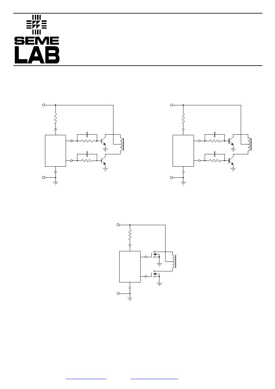
APPLICATIONS INFORMATION
14
A
B
IP1526
+V
C
GND
15
13
16
+V
SUPPLY
R1
RETURN
R2
C2
R3
C1
Q1
Q2
T1
14
A
B
IP1526
+V
C
GND
15
13
16
+V
SUPPLY
R1
RETURN
R2
C2
R3
C1
Q1
Q2
T1
Push≠Pull Configuration
Driving N≠Channel Power MOSFETs
Single≠Ended Configuration
IP1526 SERIES
4/99
Semelab plc.
Telephone +44(0)1455 556565. Fax +44(0)1455 552612.
E-mail:
sales@semelab.co.uk
Website:
http://www.semelab.co.uk
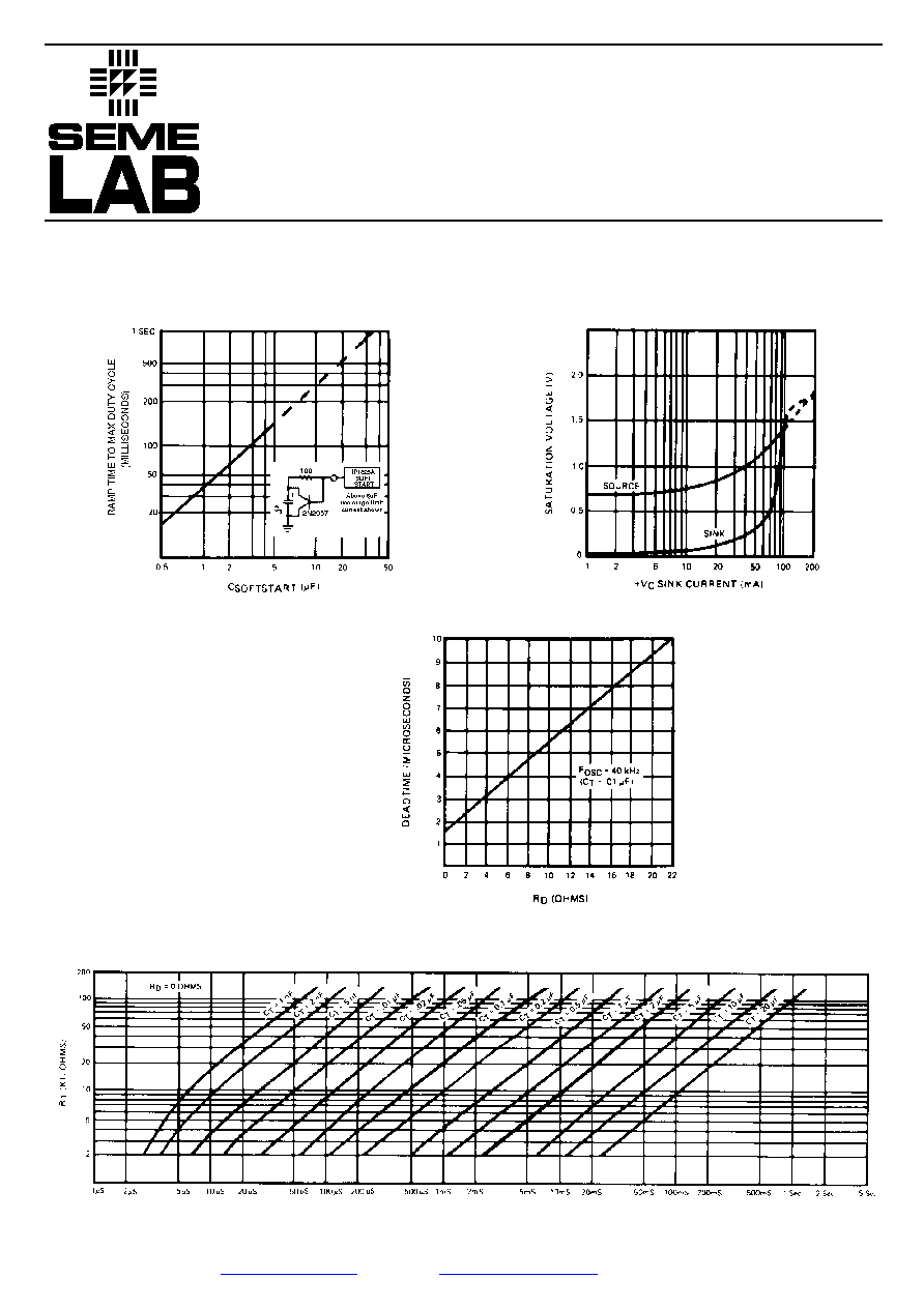
TYPICAL PERFORMANCE CHARACTERISTICS
Soft Start Time vs C
S
Output Driver Saturation Voltage
Output Driver Deadtime vs R
D
Value
Oscillator Period vs R
T
and C
T