LAB
SEME
IP1844 SERIES
IP1845 SERIES
Semelab plc.
Telephone (01455) 556565. Telex: 341927. Fax (01455) 552612.
Prelim. 2/95
CURRENT MODE
REGULATING
PULSE WIDTH
MODULATORS
FEATURES
∑ Guaranteed ±1% reference voltage tolerance
∑ Guaranteed ±10% frequency tolerance
∑ Low start≠up current (<500
m
A)
∑ Under voltage lockout with hysteresis
∑ Output state completely defined for all supply
and input conditions
∑ Interchangeable with UC1844 and UC1845
series for improved operation
∑ 500kHz Oscillator operation
250kHz Output operation
+30V
Self limiting
±1A
5
µ
J
≠0.3V to +V
CC
10mA
1W
10mW/∞C
725mW
7.25mW/∞C
2W
16mW/∞C
≠65 to 150∞C
+300∞C
ABSOLUTE MAXIMUM RATINGS
(T
case
= 25∞C unless otherwise stated)
TOP VIEW
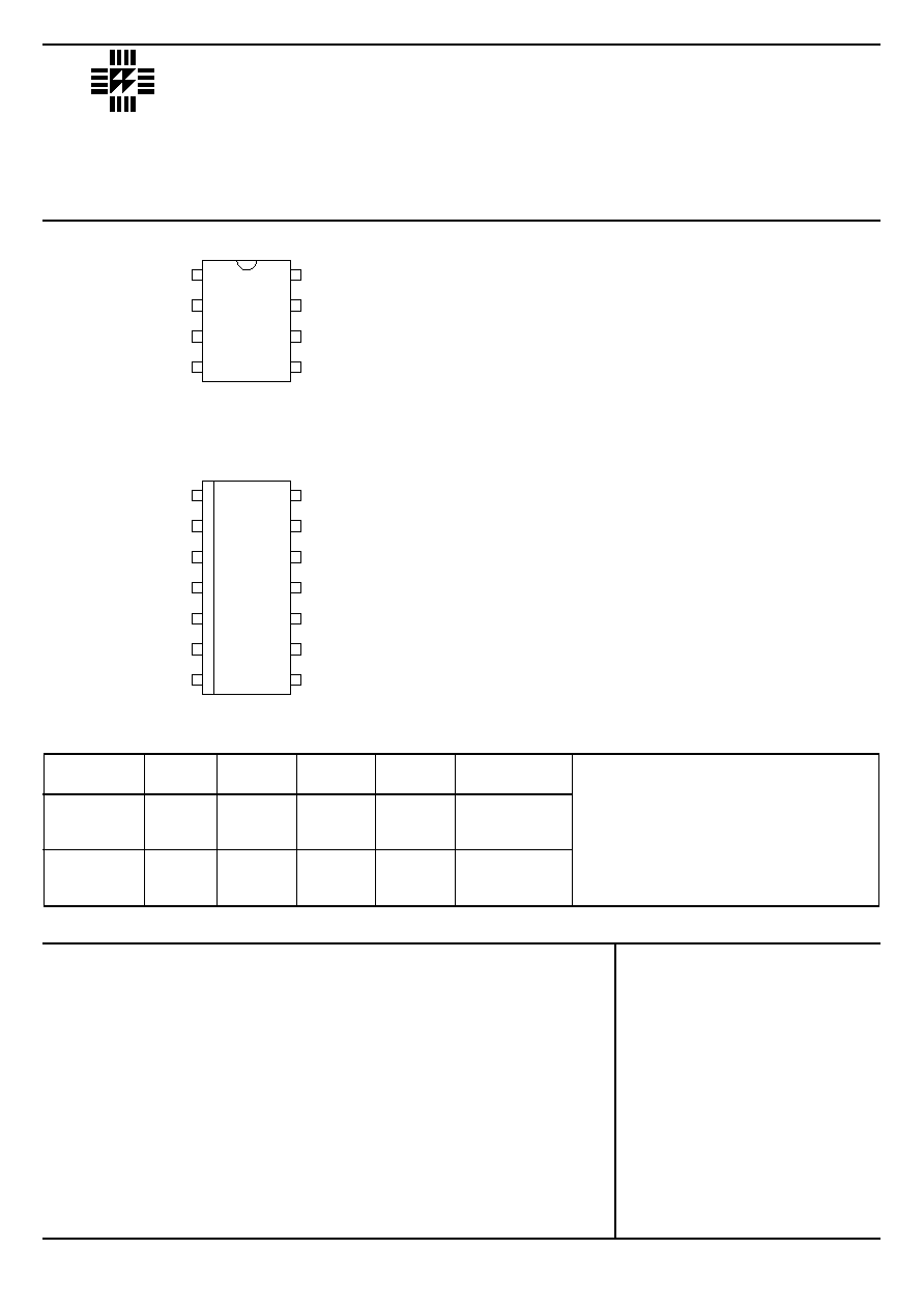
J Package ≠ 8 Pin Ceramic DIP
N Package ≠ 8 Pin Plastic DIP
D-8 Package ≠ 8 Pin Plastic (150) SOIC
1
2
3
4
8
7
6
5
COMP
V
REF
GROUND
OUTPUT
R
T
/C
T
V
CC
I
SENSE
V
FB
TOP VIEW
D-14 Package ≠ 14 Pin Plastic (150) SOIC
COMP
V
REF
GROUND
OUTPUT
1
2
3
4
POWER
GROUND
5
6
7
14
13
12
11
10
9
8
N/C
R
T
/C
T
I
SENSE
N/C
N/C
N/C
V
CC
V
FB
V
C
V
CC
Supply Voltage
(low impedance source)
(I
CC
< 30mA)
I
O
Output Current
Output Energy
(capacitive load)
Analog Inputs
(pins 2 and 3)
Error Amp Output Sink Current
P
D
Power Dissipation
T
amb
= 25∞C
J, N Packages
Derate @ T
amb
> 50∞C
P
D
Power Dissipation
T
case
= 25∞C
D Package
Derate @ T
amb
> 50∞C
P
D
Power Dissipation
T
case
= 25∞C
J, N Packages
Derate @ T
case
> 25∞C
T
STG
Storage Temperature Range
T
L
Lead Temperature
(soldering, 10 seconds)
Part J≠Pack
N≠Pack
D≠8
D≠14
Temp.
Number
8 Pin
8 Pin
8 Pin
14 Pin
Range
IP1844
-55 to +125∞C
IP2844
-25 to +85∞C
IP3844
0 to +70∞C
IP1845
-55 to +125∞C
IP2845
-25 to +85∞C
IP3845
0 to +70∞C
Order Information
Note:
To order, add the package identifier to the
part number.
eg.
IP1844D≠14
IP3845J
LAB
SEME
IP1844 SERIES
IP1845 SERIES
Semelab plc.
Telephone (01455) 556565. Telex: 341927. Fax (01455) 552612.
Prelim. 2/95
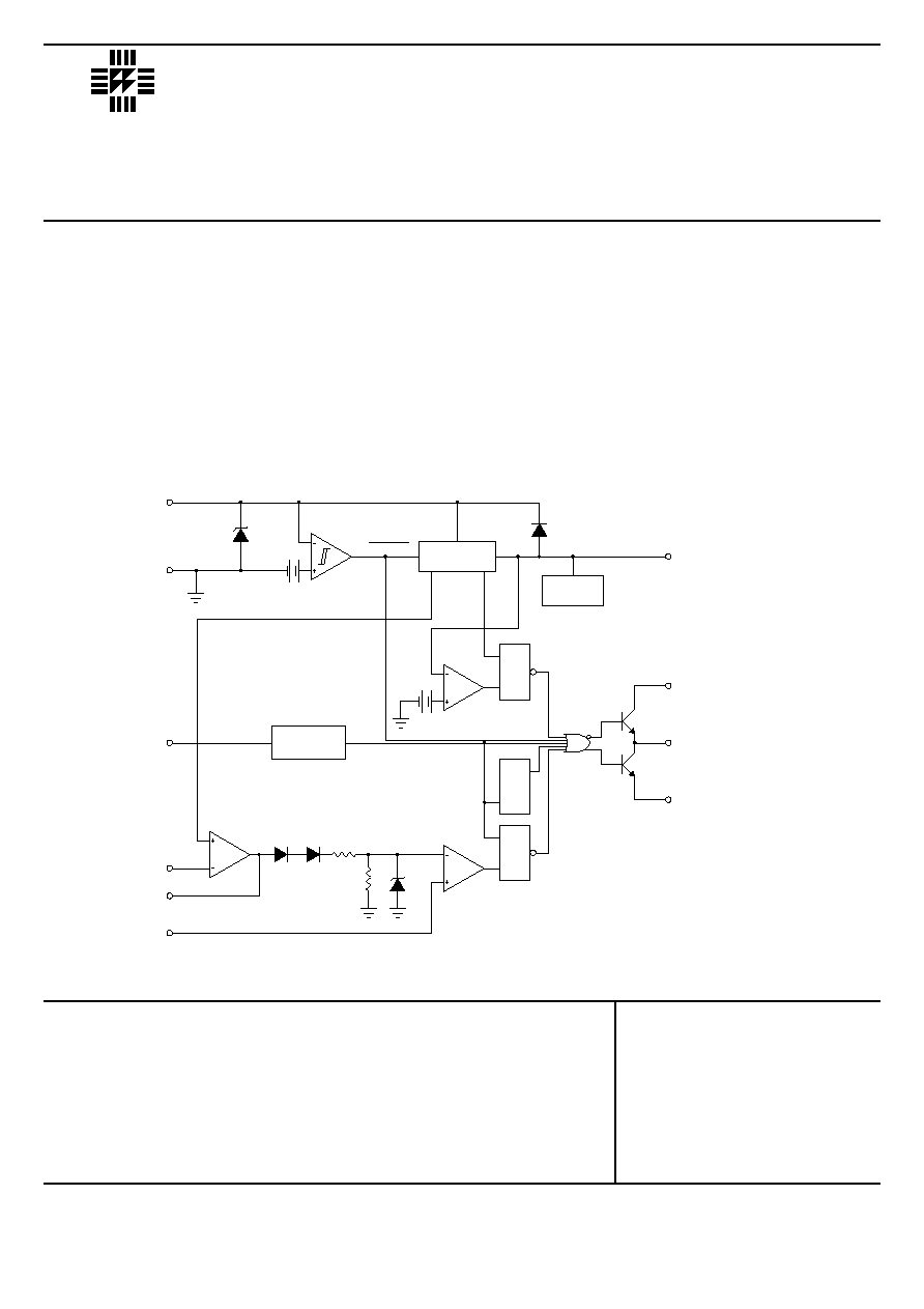
DESCRIPTION
The IP1844 and IP1845 series of switching regulator control circuits contain all the functions necessary to
implement off-line, current mode switching regulators, using a minimum number of external parts.
Functions included are voltage reference, error amplifier, current sense comparator, oscillator, totem-pole output
driver and under-voltage lockout circuitry. In addition there is a toggle flip-flop which blanks the output on every
second clock pulse, thereby ensuring that the duty cycle never exceeds 50%.
Although pin compatible with the UC1844 and UC1845 series, SEMELAB has incorporated several improvements
in the IP1844 and IP1845 series allowing tighter and more complete specification of electrical performance .
BLOCK DIAGRAM
Values in brackets are for IP1845 series.
3.6V
ERROR
AMP
OSCILLATOR
2R
R
1V
R
S
PW M
LATCH
CURRENT
SENSE
COM PARATOR
16V
(8.4V)
6V
(0.5V)
2.5V
UNDER≠VOLTAGE
LOCKOUT
ENABLE
REFERENCE
REGULATOR
5V
INTERNAL
BIAS
34V
REG
R
S
V STATUS
LATCH
REF
T
Q
TOGGLE
FLIP
FLOP
PIN NUM BERS
1st Num ber
2nd Num ber
≠ N, J and 8 Pin D Packages
≠ 14 Pin D Package.
C
OMP
G
ND
V
CC
I
SENSE
V
FB
/C
R
T
T
OUTPUT
POW ER
GROUND
V
REF
V
C
3/5
5/9
7/12
2/3
1/1
4/7
6/10
7/11
5/8
8/14
V
CC
Supply Voltage
I
O
Output Current
Analog Inputs
(pins 2 and 3)
Error Amp Output Sink Current
IP1844 , IP1845
Operating Ambient Temperature Range
IP2844 , IP2845
IP3844 , IP3845
30V
0 to ±200mA
≠0.3V to 3V
0 to 2mA
≠55 to 125∞C
≠25 to 85∞C
0 to 70∞C
RECOMMENDED OPERATING CONDITIONS
LAB
SEME
IP1844 SERIES
IP1845 SERIES
Semelab plc.
Telephone (01455) 556565. Telex: 341927. Fax (01455) 552612.
Prelim. 2/95
4.90
5.00
5.10
6
20
6
25
0.2
0.4
4.82
5.18
50
5
25
30
80
160
47
52
57
0.2
1
5
1.7
8.3
8
2.42
2.50
2.58
≠0.3
≠2
65
90
0.7
1
60
70
2
6
≠0.5
≠0.8
5.0
6.0
0.7
1.1
4.95
5.00
5.05
6
20
6
25
0.2
0.4
4.90
5.10
50
5
25
30
80
160
47
52
57
0.2
1
5
1.7
8.3
8
2.45
2.50
2.55
≠0.3
≠1
65
90
0.7
1
60
70
2
6
≠0.5
≠0.8
5.0
6.0
0.7
1.1
IP1844/IP1845
IP3844
IP2844/IP2845
IP3845
Parameter
Test Conditions
Min.
Typ.
Max.
Min.
Typ.
Max.
Units
Output Voltage
Input Regulation
Output Regulation
Temperature Stability
Total Output Variation
Output Noise Voltage
Long Term Stability
Output Short Circuit
Current
Frequency
Voltage stability
Temperature Stability
Amplitude
Discharge Current
Input Voltage
Input Bias Current
Open Loop Voltage
Gain
Unity Gain Bandwidth
Supply Voltage
Rejection
Output Sink Current
Output Source Current
V
OUT
High
V
OUT
Low
I
O
= 1mA
T
J
= 25∞C
V
CC
= 12V to 25V
I
O
= 1mA to 20mA
Line, Load, Temp
f = 10Hz to 10kHz
T
J
= 25∞C
T
J
= 125∞C @ 1000Hrs
V
REF
= 0
T
J
= 25∞C
V
CC
= 12V to 25V
T
A
= Min to Max
V
PIN4
Peak to Peak
T
J
= 25∞C
T
A
= Min to Max
V
PIN1
= 2.5V
V
O
= 2V to 4V
V
CC
= 12V to 25V
V
PIN2
= 2.7V
V
PIN1
= 1.1V
V
PIN2
= 2.3V
V
PIN1
= 5.0V
V
PIN2
= 2.3V
R
L
= 15k
V
PIN2
= 2.7V
R
L
= 15k
V
mV
mV
∞C
V
µ
V
mV
mA
kHz
%
%
V
mA
%
V
µ
A
dB
MHz
dB
mA
V
ELECTRICAL CHARACTERISTICS
(Over Full Operating Temperature Range unless otherwise stated)
REFERENCE SECTION
OSCILLATOR SECTION
ERROR AMP SECTION
NOTES
1. Test Conditions unless otherwise stated:
V
CC
= 15V* , R
T
= 10k
, C
T
= 3.3nF , f = 52kHz.
*Adjust V
CC
above start threshold before setting at required level.
All specifications apply over the full operating temperature range
unless otherwise stated. (See Ordering Information for further details).
IP1844/IP1845
IP3844
IP2844/IP2845
IP3845
Parameter
Test Conditions
Min.
Typ.
Max.
Min.
Typ.
Max.
Units
2.85
3
3.15
0.9
1
1.1
60
70
≠2
≠10
150
300
0.1
0.4
1.5
2.2
13
13.5
12
13.5
50
150
50
150
0.7
1.1
14.5
16
17.5
7.8
8.4
9
8.5
10
11.5
7
7.6
8.2
0.3
0.5
11
15
14
17
30
34
40
46
48
50
0
2.85
3
3.15
0.9
1
1.1
60
70
≠2
≠10
150
300
0.1
0.4
1.5
2.2
13
13.5
12
13.5
50
150
50
150
0.7
1.1
15
16
17
7.8
8.4
9
9
10
11
7
7.6
8.2
0.3
0.5
11
15
14
17
30
34
40
47
48
50
0
Gain
Maximum Input Signal
Supply Voltage
Rejection
Input Bias Current
Delay to Output
Output Low Level
Output High Level
Rise Time
Fall Time
UVLO Saturation
Upper Threshold
(V
CC
)
Lower Threshold
(V
CC
)
Start≠up Current
Operating Supply
Current
V
CC
Zener Voltage
Maximum Duty Cycle
Minimum Duty Cycle
See Notes 2,3
V
PIN1
= 5.0V
(Note 2)
V
C
= 12V to 25V
I
SINK
= 20mA
I
SINK
= 200mA
I
SOURCE
= 20mA
I
SOURCE
= 200mA
C
L
= 1nF
C
L
= 1nF
V
CC
= 6V
I
L
= 1mA
1844 Series
1845 Series
1844 Series
1845 Series
V
PIN2
= 0V
1844 Series
V
PIN3
= 0V
1845 Series
I
CC
= 25mA
V/V
V
dB
µ
A
ns
V
V
ns
V
V
V
mA
mA
V
%
LAB
SEME
IP1844 SERIES
IP1845 SERIES
Semelab plc.
Telephone (01455) 556565. Telex: 341927. Fax (01455) 552612.
Prelim. 2/95
ELECTRICAL CHARACTERISTICS
(Over Full Operating Temperature Range unless otherwise stated)
CURRENT SENSE SECTION
OUTPUT SECTION
UNDER≠VOLTAGE LOCKOUT SECTION
PWM SECTION
NOTES
1. Test Conditions unless otherwise stated:
V
CC
= 15V* , R
T
= 10k
, C
T
= 3.3nF , f = 52kHz.
*Adjust V
CC
above start threshold before setting at
required level.
All specifications apply over the full operating temperature
range unless otherwise stated.
(See Ordering Information for further details).
2. Parameter measured at trip point of latch with
V
PIN2
= 0V
3. Gain defined as:
V
PIN1
A =
V
PIN3
0
V
PIN3
0.8
TOTAL STANDBY CURRENT
LAB
SEME
IP1844 SERIES
IP1845 SERIES
Semelab plc.
Telephone (01455) 556565. Telex: 341927. Fax (01455) 552612.
Prelim. 2/95
APPLICATIONS INFORMATION
V - Pin 4
(Pin 7 for 14 Pin D Package)
8
4
5
GND
REF
V
R C
T
T
C
T
R
T
Internal Clock
Internal Clock
Output ≠ Max. Duty Cycle
V - Pin 6
(Pin 10 for 14 Pin D Package)
Output ≠ Max. Duty Cycle
V - Pin 6
(Pin 10 for 14 Pin D Package)
V - Pin 4
(Pin 7 for 14 Pin D Package)
LARGE
SMALL
R
T
C
T
LARGE
SMALL
R
T
C
T
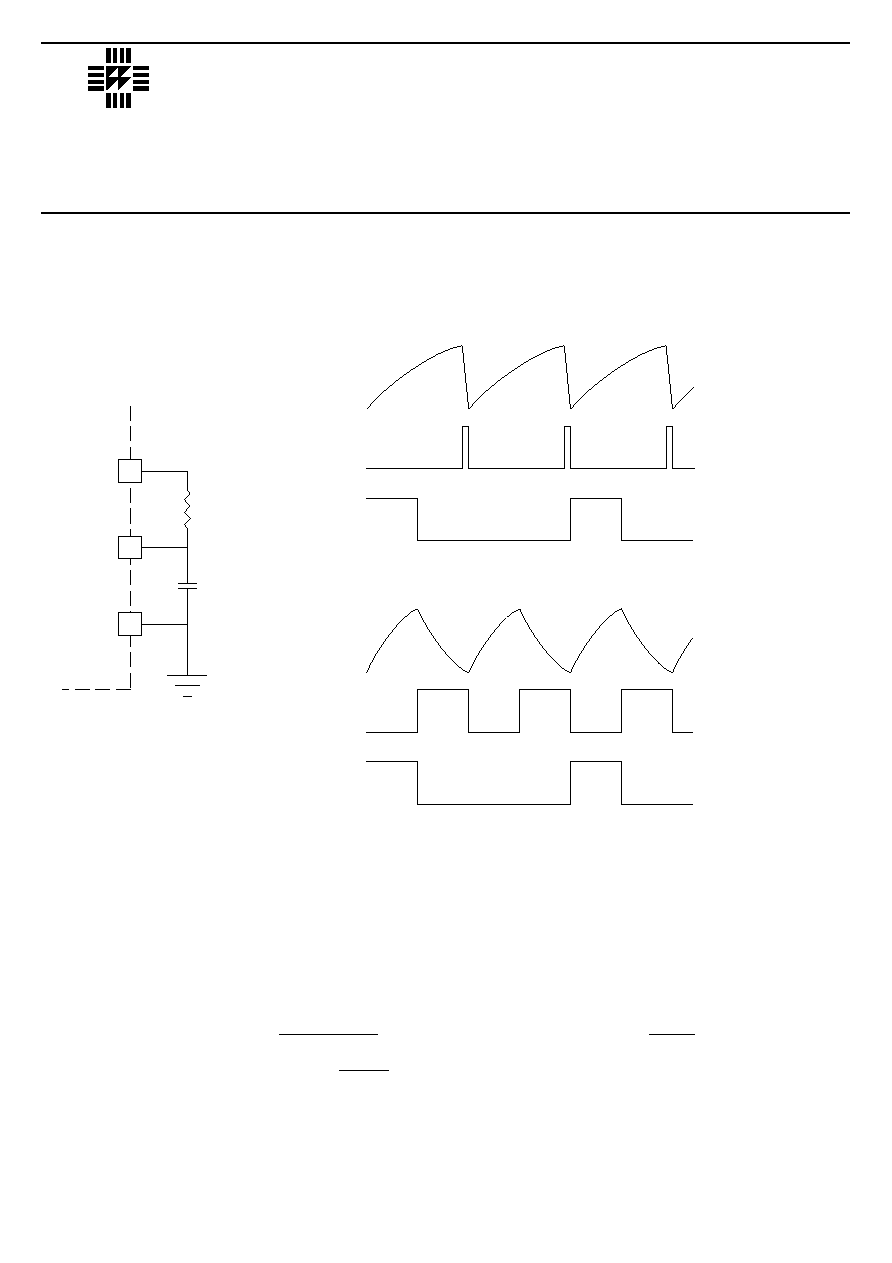
Oscillator Waveforms and Maximum Duty Cycle
Oscillator timing capacitor C
T
is charged by V
REF
through R
T
and discharged by an
internal current source. During the discharge time, the internal clock signal blanks the
output to the low state. Selection of R
T
and C
T
therefore determines both oscillator
frequency and maximum duty cycle.
Charge and discharge times are determined by the formulae:
t
c
0.55 R
T
C
T
t
d
R
T
C
T
R
n
1
Resultant frequency f =
(t
c
+ t
d
)
For R
T
> 5k
,
1.8
Resultant frequency f
(R
T
C
T
)
.0063 R
T
≠ 2.3
.0063 ≠ 4
( )
LAB
SEME
IP1844 SERIES
IP1845 SERIES
Semelab plc.
Telephone (01455) 556565. Telex: 341927. Fax (01455) 552612.
Prelim. 2/95
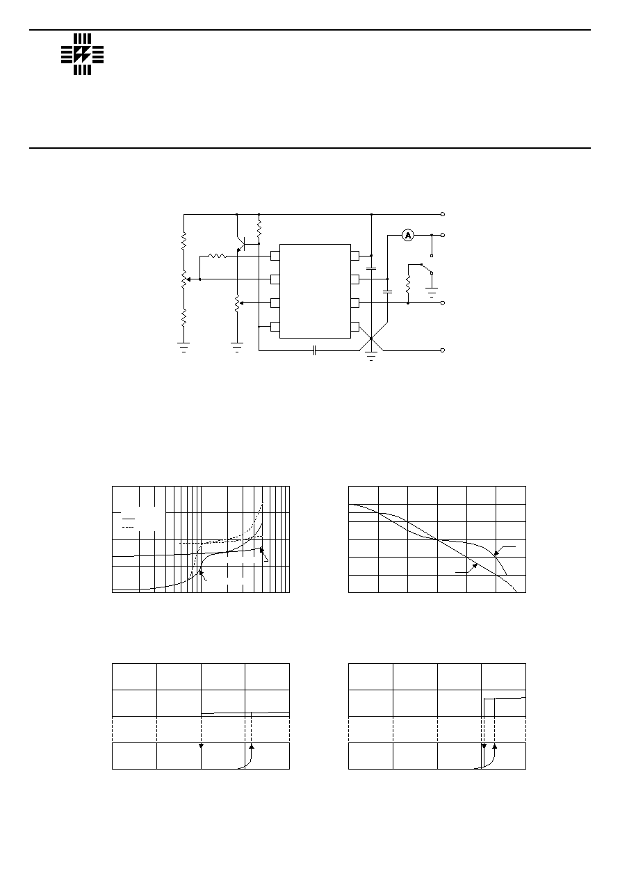
Open≠Loop Laboratory Test Fixture
.01
.02
.04
.07
.1
.2
.4
.7
1.0
4
3
2
1
0
60
40
20
0
100
80
10
1k
100
10k
10M
100k
1M
.05
.5
.03
.3
OUTPUT CURRENT, SOURCE / SINK (A)
FREQUENCY (Hz)
SAT
U
R
A
T
I
O
N
VO
L
T
AG
E
(
V
)
VO
L
T
AG
E G
A
I
N
(
d
B)
OUTPUT SATURATION CHARACTERISTICS
ERROR AMPLIFIER OPEN-LOOP
FREQUENCY RESPONSE
V = 15V
CC
T = 25∞C
A
A
V
B
SOURCE SAT
V - )
CC
V
OH
S INK SAT (V )
OL
(
A
T = ≠55∞C
≠45
≠90
≠135
≠180
0
PH
ASE
(
∞
)
TYPICAL PERFORMANCE CHARACTERISTICS
APPLICATIONS INFORMATION
High peak current associated with capacitive loads necessitate careful grounding techniques. Timing and bypass capacitors should
be connected close to pin 5 in a single point ground. The transistor and 5K potentiometer are used to sample the oscillator wave
form and apply an adjustable ramp to pin 3.
0.1
µ
F
1k
1kW
1k
ERROR AMP
ADJUST
4.7k
5k
ADJUST
4.7k
100k
2N2222
I
SENSE
R
T
C
T
0.1
µ
F
V
REF
V
CC
OUTPUT
GROUND
1
2
4
5
7
8
3
6
I
SENSE
V
REF
V
CC
O/P
GND
COMP
V
FB
R
T
/C
T
0
20
15
10
0.5
0
10
5
15
20
0
20
15
10
0.5
0
5
2.5
7.5
10
UNDER VOLTAGE LOCKOUT
1844 SERIES
UNDER VOLTAGE LOCKOUT
1845 SERIES
V (V)
CC
I
(
m
A
)
CC
V (V)
CC
I
(
m
A
)
CC