 | –≠–ª–µ–∫—Ç—Ä–æ–Ω–Ω—ã–π –∫–æ–º–ø–æ–Ω–µ–Ω—Ç: IP1M12D | –°–∫–∞—á–∞—Ç—å:  PDF PDF  ZIP ZIP |
LAB
SEME
IP1M10 SERIES
IP1M12 SERIES
Semelab plc.
Telephone (01455) 556565. Telex: 341927. Fax (01455) 552612.
Prelim. 7/95
200mA DUAL H-BRIDGE
FEATURES
∑ 200mA Continuous output current per bridge
(100mA for IP1Mxx, IP2Mxx)
∑ Internal output clamp diodes
∑ Hysteretic logic inputs for noise immunity
∑ Thermal shutdown protection
∑ Peak current limit protection
∑ Crossover current blanking
∑ Separate +5V logic supply for minimum power
dissipation (1M10 series only)
∑ Separate +7V to +36V logic supply
(1M12 series only)
V
SS
Logic Supply Voltage
1M10 Series
1M12 Series
V
C
Driver Supply Voltage
Logic Inputs
Output Current
Peak Output Current
P
D
Power Dissipation
T
A
= 25∞C
Derate above 50∞C
P
D
Power Dissipation
T
C
= 25∞C
Derate above 25∞C
T
J
Operating Junction Temperature
T
STG
Storage Temperature Range
+7V
+40V
+40V
-0.3 to +40V
±250mA
Internally Limited
1W
10mW/∞C
2W
16mW/∞C
See Ordering Information
≠65 to +150∞C
ABSOLUTE MAXIMUM RATINGS
(T
case
= 25∞C unless otherwise stated)
TOP VIEW
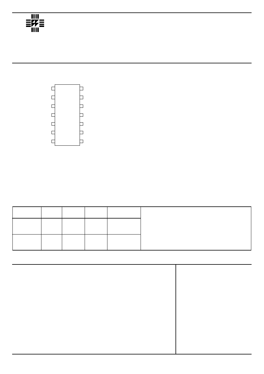
J Package ≠ 14 Pin Ceramic DIP
N Package ≠ 14 Pin Plastic DIP
D Package ≠ 14 Pin Plastic (150) SOIC
9
1 0
8
1
2
3
4
5
6
7
1 4
1 3
1 2
1 1
O A
+V
C A
V
S S
V
P W M B
DIR B
O B
+V
C B
V
O B
≠V
E B
V
G N D
DIR A
P W M A
E A
V
O A
≠V
Part J≠Pack
N≠Pack
D≠14
Temp.
Number
14 Pin
14 Pin
14 Pin
Range
IP1M10
-55 to +125∞C
IP2M10
-40 to +85∞C
IP3M10
0 to +70∞C
IP1M12
-55 to +125∞C
IP2M12
-40 to +85∞C
IP3M12
0 to +70∞C
Order Information
Note:
To order, add the package identifier to the part number.
eg.
IP1M10J
IP2M10D≠14
IP3M12N
LAB
SEME
IP1M10 SERIES
IP1M12 SERIES
Semelab plc.
Telephone (01455) 556565. Telex: 341927. Fax (01455) 552612.
Prelim. 7/95
INTERNAL
BIASING
12
PWM
A
11
DIR
A
5
DIR
B
CB
V
6
25
25
14
≠V
OA
1
OA
+V
7
OB
+V
8
OB
≠V
EA
V
13
CA
V
2
3
SS
V
4
PWM
B
GND
10
EB
V
9
V
SS
Logic Supply Voltage
1M10 Series
1M12 Series
V
C
Driver Supply Voltage
Logic Inputs
Output Current, DC
1Mxx / 2Mxx Series
3Mxx Series
Peak Output Current
1Mxx / 2Mxx Series
3Mxx Series
T
AMB
Operating Ambient Temperature Range
1Mxx Series
2Mxx Series
3Mxx Series
+4.75 to +5.25V
+7 to +36V
+4.75 to +36V
0 to +36V
±100mA
±200mA
±125mA
±250mA
-55 to +125∞C
-40 to +85∞C
0 to +70∞C
RECOMMENDED OPERATING CONDITIONS
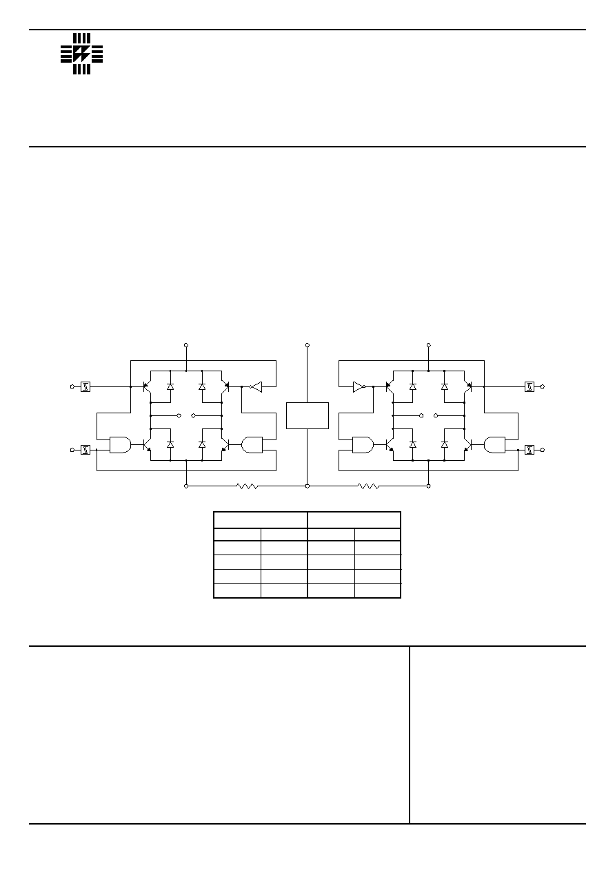
BLOCK DIAGRAM
DESCRIPTION
The IP1M10 and IP1M12 series each contain two full H-bridge power drivers capable of delivering 200 mA continuous
output current per channel (100mA for 1Mxx / 2Mxx). Each bridge may be run from its own supply voltage of up to 36V
and is controlled by 2 high voltage protected logic level inputs with internal hysteresis for noise immunity.
Protection features include thermal shutdown, peak current limiting, crossover current blanking, and internal output
clamp diodes. Logic supply current is provided by a separate pin so that standby power dissipation may be minimised.
The IP1M10 series requires a +5V logic supply while the IP1M12 series requires a logic supply voltage of +7V or greater,
and is typically used in single supply applications.
The IP1M10 and IP1M12 are available in a 14 lead ceramic DIP while the IP2M10, IP2M12, IP3M10, IP3M12 are avail-
able in the 14 lead ceramic DIP, 14 lead plastic DIP, and 14 lead plastic SOIC packages.
INPUTS
OUTPUTS
DIR
PWM
+V
O
-V
O
LOW
LOW
HIGH
HIGH
LOW
HIGH
LOW
HIGH
Z*
LOW
HIGH
HIGH
HIGH
HIGH
Z*
LOW
* Z = High Impedance.
LAB
SEME
IP1M10 SERIES
IP1M12 SERIES
Semelab plc.
Telephone (01455) 556565. Telex: 341927. Fax (01455) 552612.
Prelim. 7/95
Logic Supply Voltage
(Pin 3)
Logic Supply Voltage
(Pin 3)
Quiescent Bridge Current (Pin 2 or 6)
PWM Input Threshold
(Pins 4 and 12)
PWM Input Current
(Pins 4 and 12)
DIR Input Threshold
(Pins 5 and 11)
DIR Input Current
(Pins 5 and 11)
Total Saturation Voltage
V
SAT(SINK)
+ V
SAT(SOURCE)
Diode Forward Voltage
Output Leakage Current
(Pins 1, 7, 8 and 14)
V
SS
= +5.25V
I
LOADS
= 0
V
SS
= +5.25V
I
LOADS
= 100mA
V
SS
= +5.25V
I
LOADS
= 200mA
V
SS
= +36V
I
LOADS
= 0
V
SS
= +36V
I
LOADS
= 100mA
V
SS
= +20V
I
LOADS
= 200mA
I
LOAD
= 0
V
IN
= 0
V
IN
= 36V
V
IN
= 0
V
IN
= 36V
I
LOAD
= 100mA
I
LOAD
= 200mA
3M10 / 3M12 Only
I
DIODE
= 100mA
I
DIODE
= 200mA
V
O
= 0
V
C
= 36V
V
O
= V
C
= 36V
5
12
8
20
12
28
8
18
1
25
15
32
2.5
8
0.8
1.5
2
1.2
2.5
3
0.4
1
-20
-100
0.1
±10
0.8
1.5
2
1.2
2.3
3
0.2
0.8
-20
-100
0.1
±10
1.8
2.25
2.1
2.7
1.1
1.4
1.2
1.6
1
100
1
100
Parameter
Test Conditions
Min.
Typ.
Max.
Units
ELECTRICAL CHARACTERISTICS
(Over Full Operating Temperature Range)
mA
mA
V
µ
A
V
µ
A
V
V
µ
A
1M10 Series
1M12 Series
Falling
Rising
Hysterisis
Low
High
Falling
Rising
Hysterisis
Low
High
Low
High
Sink Turn-On Delay
Sink Current Rise Time
Sink Turn-Off Delay
Sink Current Fall Time
Source Turn-On Delay
Source Rise Time
Source Turn-Off Delay
Source Fall Time
Sink to Source Deadtime
Source to Sink Deadtime
t: V
i
= V
i(TH)
to V
O
= V
S
/2
t: I
O
= (0.1 to 0.9) I
LOAD
t: V
i
= V
i(TH)
to V
O
= V
S
/2
t: I
O
= (0.9 to 0.1) I
LOAD
t: V
i
= V
i(TH)
to V
O
= V
S
/2
t: I
O
= (0.1 to 0.9) I
LOAD
t: V
i
= V
i(TH)
to V
O
= V
S
/2
t: I
O
= (0.9 to 0.1) I
LOAD
1250
200
300
200
800
400
1000
500
500
250
Parameter
Test Conditions
Min.
Typ.
Max.
Units
SWITCHING CHARACTERISTICS
@ T
AMB
= 25∞C
ns
ns
ns
LAB
SEME
IP1M10 SERIES
IP1M12 SERIES
Semelab plc.
Telephone (01455) 556565. Telex: 341927. Fax (01455) 552612.
Prelim. 7/95
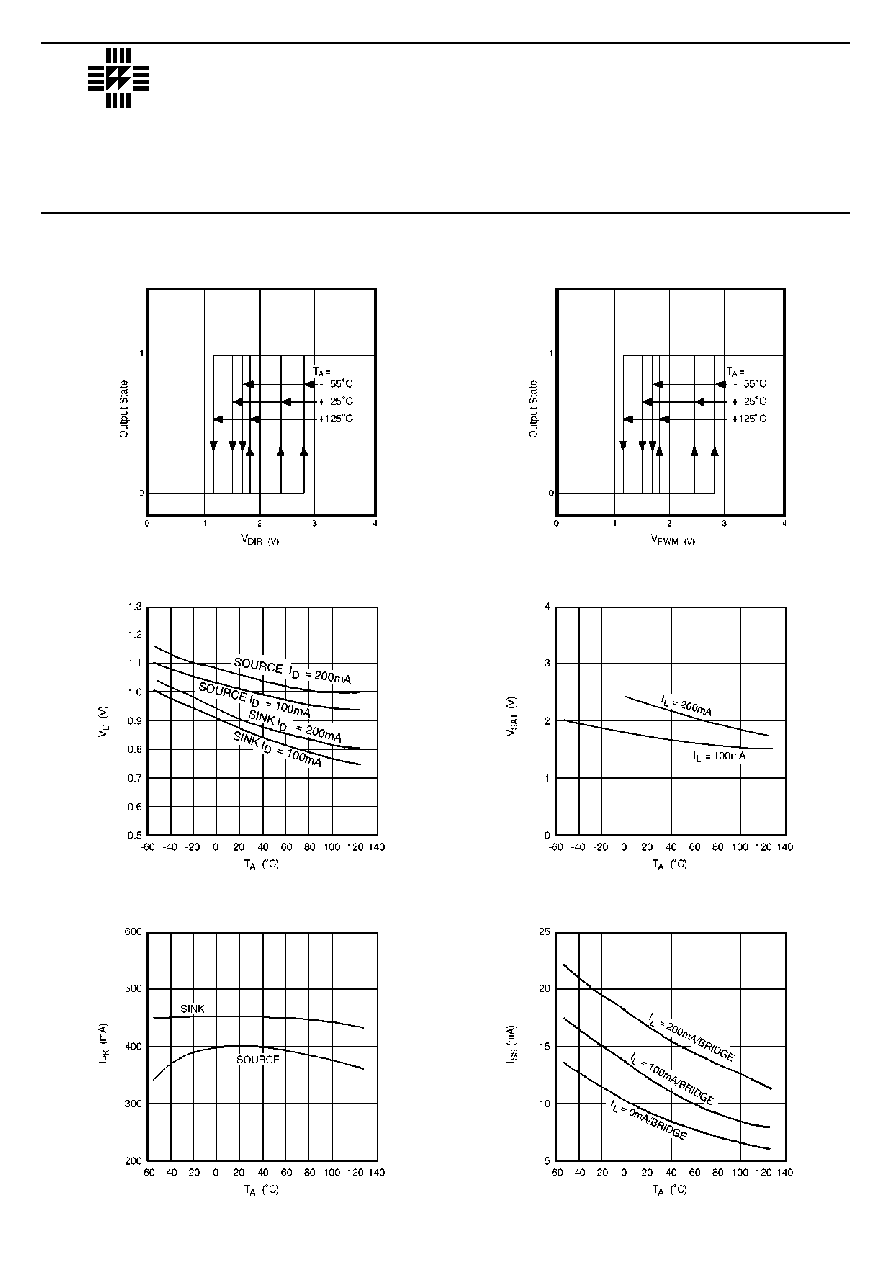
TYPICAL PERFORMANCE CHARACTERISTICS -- ERROR AMPLIFIER
Output State vs DIR Input Voltage
Output State vs PWM Input Voltage
Diode Forward Voltage vs
Ambient Temperature
Total Saturation Voltage vs
Ambient Temperature
Peak Output Current vs
Ambient Temperature
Logic Supply Current vs
Ambient Temperature