 | –≠–ª–µ–∫—Ç—Ä–æ–Ω–Ω—ã–π –∫–æ–º–ø–æ–Ω–µ–Ω—Ç: IP1P125 | –°–∫–∞—á–∞—Ç—å:  PDF PDF  ZIP ZIP |
IP1P125
IP3P125
Prelim.5/00
Semelab plc.
Telephone +44(0)1455 556565. Fax +44(0)1455 552612.
E-mail:
sales@semelab.co.uk
Website:
http://www.semelab.co.uk
REGULATING PULSE
WIDTH MODULATORS
FEATURES
∑ Pin Compatible with 1525A Series
∑ Low Output Crossover Current
∑ Fixed 100ns Deadtime
∑ 100Hz to 500kHz Operating Frequencyrange
∑ 5.1 volt ± 1% Reference
∑ Oscillator Sync. Terminal
∑ Soft Start
∑ Undervoltage Lockout
∑ Latching PWM
+V
IN
Input Voltage
Collector Voltage
Logic Inputs
Analogue Inputs
Output Current, Source or Sink
Reference Output Load Current
Oscillator Charging Current
P
D
Power Dissipation
T
A
= 25∞C
Derate @ T
A
> 50∞C
P
D
Power Dissipation
T
C
= 25∞C
Derate @ T
C
> 25∞C
T
J
Operating Junction Temperature
T
STG
Storage Temperature Range
T
L
Lead Temperature
(soldering, 10 seconds)
+40V
+40V
≠0.3 to +5.5V
≠0.3 to +V
IN
500mA
Internally Limited
5mA
1000mW
10mW/∞C
2000W
16mW/∞C
≠55 to +150∞C
≠65 to +150∞C
+300∞C
ABSOLUTE MAXIMUM RATINGS
(T
case
= 25∞C unless otherwise stated)
TOP VIEW
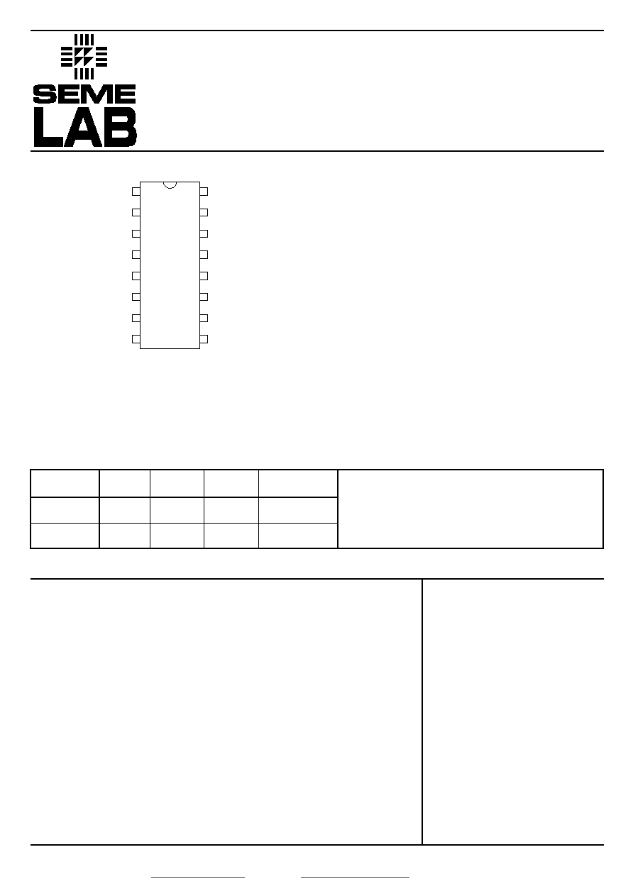
J Package ≠ 16 Pin Ceramic DIP
N Package ≠ 16 Pin Plastic DIP
D Package ≠ 16 Pin Plastic (300) SOIC
8
1
2
3
4
5
6
7
14
13
12
11
10
9
15
16
INV. INPUT
N. I. INPUT
OSC. OUTPUT
SOFT START
DISCHARGE
SYNC
V
REF
V
IN
OUTPUT B
GROUND
SHUTDOWN
COMPENSATION
C
V
OUTPUT A
C
T
R
T
Part J≠Pack
N≠Pack
D≠16
Temp.
Number
16 Pin
16 Pin
16 Pin
Range
IP1P125J
-55 to +125∞C
IP3P125D
0 to + 70∞C
IP3P125J
0 to +70∞C
IP3P125N
0 to +70∞C
Order Information
Note:
To order, add the package identifier to the part number.
eg.
IP1P125J

IP1P125
IP3P125
Prelim.5/00
Semelab plc.
Telephone +44(0)1455 556565. Fax +44(0)1455 552612.
E-mail:
sales@semelab.co.uk
Website:
http://www.semelab.co.uk
+8 to +
+4.5 to +35V
0 to 100mA
0 to 400mA
0 to 20mA
100Hz to 500kHz
1.5k
W
to 200k
W
470pF to 0.1
m
F
0 to 500
W
≠55 to +125∞C
≠25 to + 85∞C
0 to +70∞C
RECOMMENDED OPERATING CONDITIONS
V
IN
Input Voltage
Collector Voltage
Sink/Source Load Current (Steady State)
Sink/Source Load Current (Peak)
Reference Load Current
Oscillator Frequency Range
R
T
Oscillator Timing Resistor
C
T
Oscillator Timing Capacitor
Deadtime Resistor Range
Operating Ambient Temperature Range
IP1525A / IP1527A
IP2525A / IP3527A
IP3525A / IP3527A
DESCRIPTION
The IP1P125 series of pulse width modulator intergrated circuits offers high speed performance optimized for
MOSFET drive. Pin compatible with SG1525A, the IP1P125 features low crossover current through the output transistors
as well as 95% total usable output pulse width up to 500KHz. High speed latched shutdown is included as well as a pre-
cision 5.1 volt rference, error amp, oscillator, latched PWM coparator, totem-pole output drivers, soft-start and undervolt-
age lockout.

Output Voltage
Line Regulation
Load Regulation
Temperature Stability note5
Total Output
Short Circuit Current
Output Noise Voltagenote5
Long Term Stability note5
Initial Accuracy
Voltage Stability
Temperature Stability note5
Minimum Frequency
Maximum Frequency
Current Mirror
Clock Amplitude
Clock Width
Sync Threshold
Sync Input Current
Input Offset Voltage
Input Bias Current
Input Offset Current
DC Open Loop Gain
Gain Bandwidth Product
T
J
= 25∞C
V
IN
= 8 to 35V
I
L
= 0 to 20mA
Over Operating Range
V
IN
= 8 to 35V,
I
L
= 0 to 20mA
V
REF
= 0
10 Hz
£
f
£
10kHz
V
IN
= 8 to 35V
Over Operating Range
R
T
= 200k
W
C
T
= 0.1
m
F
R
T
= 2k
W
C
T
= 470pF R
D
= 0
W
I
RT
= 2mA
Output, PIN 4, C
T
= 0.1
m
F
Output, PIN 4, C
T
= 0.1
m
F
Sync Voltage = 3.5V
V
cm
= 1.5 to 5.2V
V
cm
= 1.5 to 2.5V
V
cm
= 1.5 to 5.2V
D
V
0
= 1 to 3V ,R
L
≥
10 M
W
note5
IP1P125
IP3P125
Prelim.5/00
Semelab plc.
Telephone +44(0)1455 556565. Fax +44(0)1455 552612.
E-mail:
sales@semelab.co.uk
Website:
http://www.semelab.co.uk
IP1P125
IP3P125
Parameter
Test Conditions
Min.
Typ.
Max.
Min.
Typ.
Max.
Units
ELECTRICAL CHARACTERISTICS
(T
J
= Over Operating Temperature Range unless otherwise stated)
5.0
5.1
5.2
1
15
5
25
15
20
4.95
5.25
25
70
120
40
200
1
50
37.6
40
42.4
0.1
2
1
6
80
120
900
1.7
2.0
2.2
3.0
4.0
0.3
0.5
1.0
1.2
2.0
2.8
1.0
2.5
2
10
1
10
0.1
1
60
80
1
3.5
5.05
5.10
5.15
1
10
5
15
15
50
5.0
5.2
25
70
120
40
200
1
10
37.6
40
42.4
0.1
0.5
1
4
80
120
900
1.7
2.0
2.2
3.0
4.0
0.3
0.5
1.0
1.2
2.0
2.8
1.0
2.5
0.1
5
1
10
0.1
1
60
80
1
3.5
V
mV
mV
V
mA
m
Vrms
mV
kHr
kHz
%
Hz
kHz
mA
V
m
s
V
mA
mV
m
A
dB
MHz
REFERENCE SECTION
OSCILLATOR SECTION
2
ERROR AMPLIFIER SECTION
3
V
CM
= 1.5 to 5.2V
V
IN
= 8 to 35V
V
PIN1
≠ V
PIN2
≥
150mV
V
PIN2
≠ V
PIN1
≥
150mV
Zero Duty Cycle
Max. Duty Cycle
V
SHUTDOWN
= 0V
V
SHUTDOWN
= 2V
To Outputs
V
SHUTDOWN
= 2.5V
PIN 10 to Output T
J
= 25∞C
I
SINK
= 20mA
I
SINK
= 100mA
I
SOURCE
= 20mA
I
SOURCE
= 100mA
V
C
= 35V
C
L
= 1nF
T
J
= 25∞C
C
L
= 1nF
T
J
= 25∞C
C
L
= 1nF
T
J
= 25∞C
Output Low Level
Output High Level
Common Mode Rejection
Supply Voltage Rejection
Minimum Duty Cycle
Maximum Duty Cycle
Input Threshold
Input Threshold
Input Bias Current
Soft Start Current
Soft Start Low Level
Shutdown Threshold
Shutdown Input Current
Shutdown Delay note5
Output Low Level
Output High Level
Collector Leakage Current
Rise Time
Fall Time
Dead Time
IP1P125
IP3P125
Parameter
Test Conditions
Min.
Typ.
Max.
Min.
Typ.
Max.
Units
0.2
0.5
3.8
5.6
7.0
60
90
50
60
0
45
49
0.6
0.9
3.3
3.6
50
25
50
80
0.4
0.6
0.6
1.3
2.0
0.1
1.0
50
300
0.2
0.4
1.0
2.5
18
19
17
18
200
100
300
50
300
100
0.2
0.5
3.8
5.6
7.0
60
90
50
60
0
45
49
0.6
0.9
3.3
3.6
50
25
50
80
25
50
80
0.4
0.6
0.6
1.3
2.0
0.1
1.0
50
300
0.2
0.4
0.2
0.4
1.0
2.5
18
19
17
18
200
100
300
50
300
100
V
dB
%
V
m
A
m
A
V
mA
ns
V
V
V
ns
IP1P125
IP3P125
Prelim.5/00
Semelab plc.
Telephone +44(0)1455 556565. Fax +44(0)1455 552612.
E-mail:
sales@semelab.co.uk
Website:
http://www.semelab.co.uk
NOTES
note5
These parameters, although guaranteed over the recommended conditions are not 100% tested in production.
ELECTRICAL CHARACTERISTICS
(T
J
= Over Operating Temperature Range unless otherwise stated)
PWM COMPARATOR
ERROR AMPLIFIER SECTION (cont.)
3
SHUTDOWN SECTION
OUTPUT DRIVERS (each output)
4