LAB
SEME
IP1R07A
IP3R07A
IP1R07
A
IP3R07
A
Semelab plc.
Telephone (01455) 556565. Telex: 341927. Fax (01455) 552612.
Prelim. 4/96
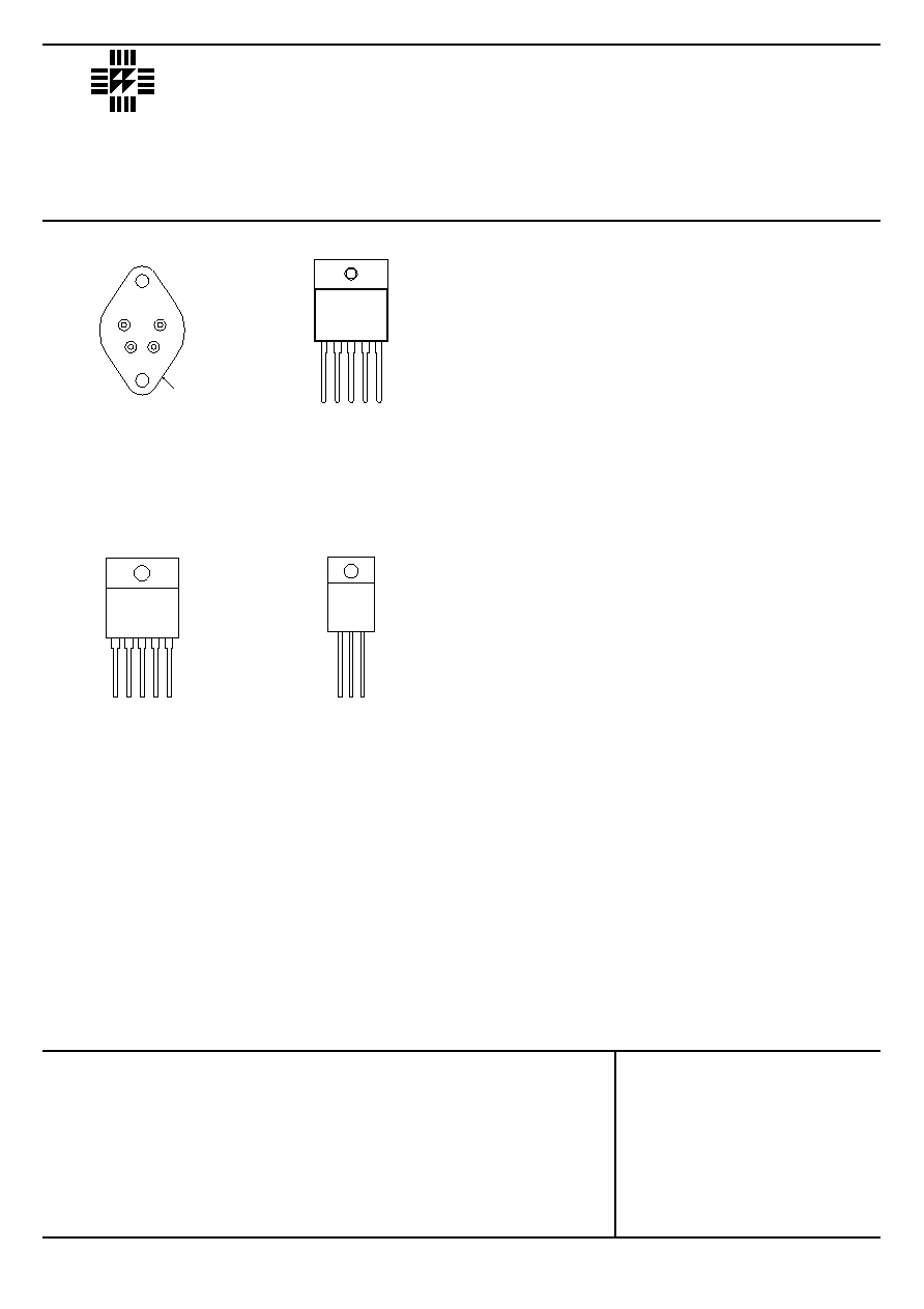
Pin 1 ≠ V
P
Pin 2 ≠ V
C
Pin 3 ≠ N/C
Pin 4 ≠ ADJ.
Case ≠ V
O
K Package ≠ TO≠3
Pin 1 ≠ V
C
Pin 2 ≠ N/C
Pin 3 ≠ V
O
Pin 4 ≠ V
P
Pin 5 ≠ ADJ.
V Package ≠ TO≠218
3 AMP
LOW DROPOUT
POSITIVE ADJUSTABLE
VOLTAGE REGULATOR
Control Input to Output Voltage
Power Input to Output Voltage
P
D
Power Dissipation
T
J
Operating Junction Temperature Range
T
STG
Storage Temperature
T
L
Lead Temperature (Soldering, 10 sec.)
35V
15V
Internally limited
See Order Information Table
≠65 to +150∞C
+300∞C
ABSOLUTE MAXIMUM RATINGS
(T
case
= 25∞C unless otherwise stated)
FEATURES
∑ 1% OUTPUT VOLTAGE TOLERANCE
(≠A VERSIONS)
∑ 0.3% LOAD REGULATION
∑ 0.01% / V LINE REGULATION
∑ 0.8V DROPOUT VOLTAGE AT 3A
∑ COMPLETE SERIES OF PROTECTIONS:
∑ CURRENT LIMITING
∑ THERMAL SHUTDOWN
∑ SOA CONTROL
1
2
5
4
3
1
2
5
3
4
Pin 1 ≠ V
C
Pin 2 ≠ N/C
Pin 3 ≠ V
O
Pin 4 ≠ V
P
Case ≠ ADJ.
T Package ≠ TO≠220
Pin 1 ≠ V
C
Pin 2 ≠ V
P
Pin 3 ≠ ADJ.
Case ≠ V
O
G Package ≠ TO≠257
3
4
5
1
2
1 2 3
Description
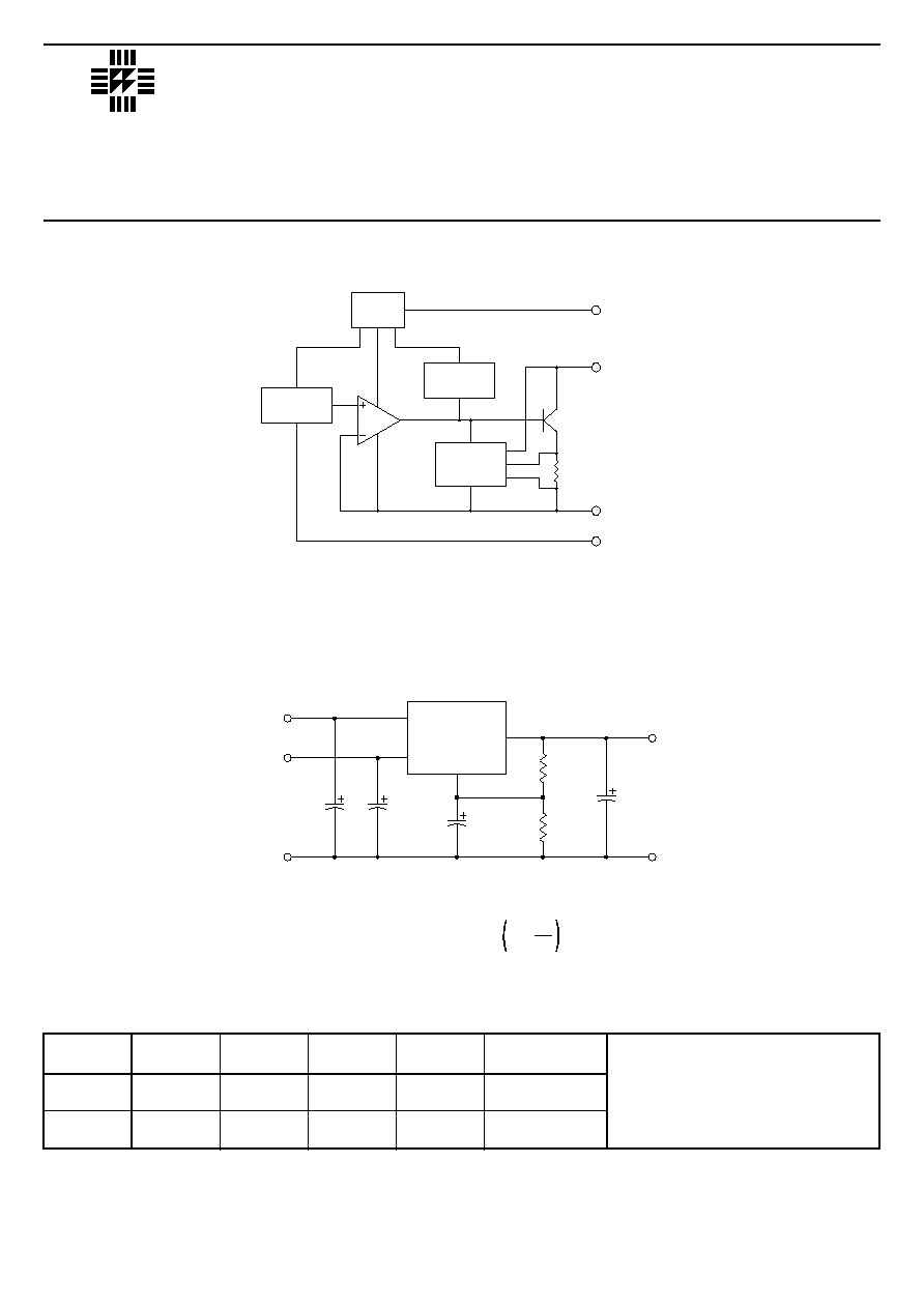
The IP3R07A series of low dropout adjustable voltage
regulators are capable of supplying 3A of output current
with an input-to-output voltage of just 0.8V. In applications
where high efficiency is necessary it is now possible to
obtain a low cost, single chip solution. These regulators
are exceptionally easy to use, requiring only two external
resistors to set the output voltage.
The IP3R07A exhibits an initial ±1% output voltage
tolerance, and over all operating conditions the reference
voltage is guaranteed not to vary more than ±2%. These
devices include internal current limiting, thermal overload
protection, and power device safe operating area
compensation.
LAB
SEME
IP1R07A
IP3R07A
IP1R07
A
IP3R07
A
Semelab plc.
Telephone (01455) 556565. Telex: 341927. Fax (01455) 552612.
Prelim. 4/96
Part K≠Pack
G≠Pack
T≠Pack
V≠Pack
Temp.
Number
(TO≠3)
(TO≠257)
(TO≠220)
(TO≠218)
Range
IP1R07A
-55 to +150∞C
IP1R07
"
IP3R07A
0 to 125∞C
IP3R07
"
Note:
To order, add the package identifier
to the part number.
eg.
IP1R07AK
Order Information
BIAS
VOLTAGE
REFERENCE
THERMAL
SHUTDOWN
CURRENT
LIMIT
POWER
INPUT
CONTROL
INPUT
INTERNAL
PASS
TRANSISTOR
CURRENT
LIMIT
SENSE
RESISTOR
A
V
OUTPUT
ADJUST
BLOCK DIAGRAM
121
ADJ
IP3R07A
1
µ
F
6V
3A
V
P
V
C
1
µ
F
10V
50mA
GND
10
µ
F *
360
1
µ
F **
5V
3A
V
O
V
OUT
Improves Ripple Rejection.
Improves Transient Response.
*
**
R1
R2
NOTE: V
O
= 1.25V 1 +
R2
R1
TYPICAL APPLICATION
LAB
SEME
IP1R07A
IP3R07A
IP1R07
A
IP3R07
A
Semelab plc.
Telephone (01455) 556565. Telex: 341927. Fax (01455) 552612.
Prelim. 4/96
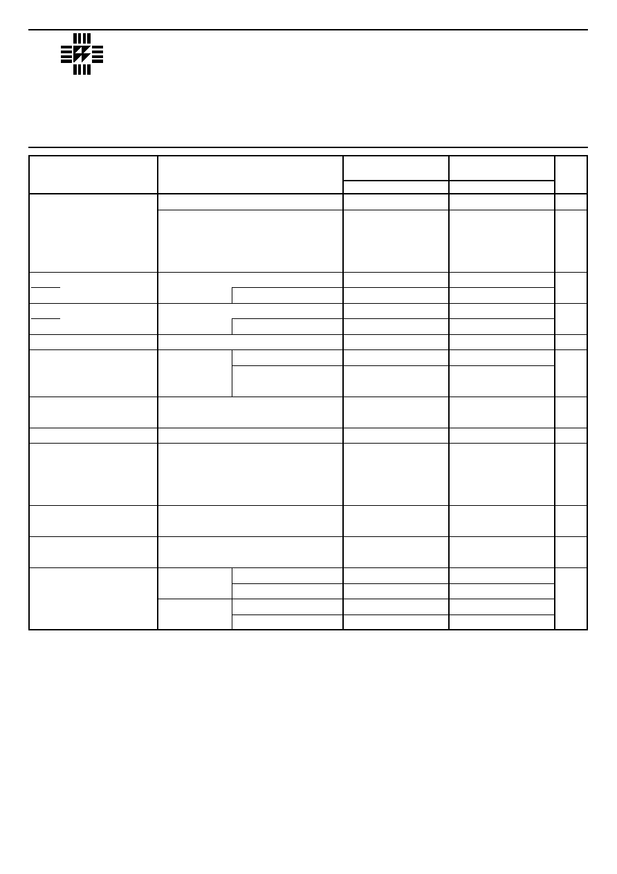
V
REF
Reference Voltage
V
OUT
Line Regulation
1
I
OUT
V
OUT
Load Regulation
1
I
OUT
Thermal Regulation
Ripple Rejection
Dropout Voltage
(Power Input)
I
ADJ
Adjust Pin Current
I
ADJ
Adjust Pin Current
Change
I
MIN
Minimum Load
Current
I
CL
Current Limit
R
JC
Thermal Resistance
Junction to Case
I
O
= 10mA
I
O
= 10mA to 3A
V
C
≠ V
O
= 3V to 35V
V
P
≠ V
O
= 1.5V to 7V
P
20W
T
J
= Over Temp. Range
1
V
C
≠ V
O
= 3V to 35V
T
J
= Over Temp. Range
1
I
O
= 10mA to 3A
T
J
= Over Temp. Range
1
t
p
= 20ms
C
ADJ
= 0
V
O
= 10V
C
ADJ
= 10
µ
F
f = 120Hz
T
J
= Over Temp. Range
1
V
O
= 50mV
T
J
= Over Temp. Range
1
I
O
= 10mA to 3A
V
P
≠ V
O
= 1.5V to 7V
V
C
≠ V
O
= 3V to 35V
T
J
= Over Temp. Range
1
V
C
≠ V
O
= 35V
T
J
= Over Temp. Range
1
V
P
≠ V
O
7V
T
J
= Over Temp. Range
1
K Package
Power Transistor
V Package
Control Circuitry
T Package
Power Transistor
G Package
Control Circuitry
1.238
1.250
1.262
1.225
1.250
1.270
0.005
0.010
0.020
0.050
0.10
0.30
0.30
1.0
0.002
0.010
65
66
86
0.8
1.0
50
100
0.2
5
3.5
5
3
4.5
1.2
0.5
2.3
0.7
1.20
1.25
1.30
0.005
0.030
0.020
0.070
0.10
0.50
0.30
1.5
0.002
0.030
65
66
86
0.8
1.0
50
100
0.2
5
3.5
10
3
4.5
1.2
0.5
2.3
0.7
V
V
% / V
%
%/W
dB
dB
V
µ
A
µ
A
mA
A
∞C/W
IP1R07A
IP1R07
IP3R07A
IP3R07
Parameter
Test Conditions
2
Min.
Typ.
Max.
Min.
Typ.
Max.
Units
Notes
1) Applies over full temperature range :≠
T
J
= ≠55 to +150∞C for IP1R07A / IP1R07
T
J
=
0 to +125∞C for IP3R07A / IP3R07
All other specifications apply at T
J
= 25∞C unless otherwise stated.
2) Test conditions unless otherwise stated :≠
V
C
- V
O
= 5V , V
P
- V
O
= 3V , I
OUT
= 3A.
Although Power Dissipation is internally limited, these specifications apply for Power Dissipation up to 50W.
3) Load and Line regulation are electrically independent and are measured using pulse techniques at low duty cycle in order to
maintain constant junction temperature. To determine the effects on the output voltage due to device heating, refer to thermal
regulation specification.