LAB
SEME
IP1R17A
IP3R17A
IP1R17
A
IP3R17
A
Semelab plc.
Telephone (01455) 556565. Telex: 341927. Fax (01455) 552612.
Prelim. 4/96
3 AMP
FIXED NEGATIVE
VOLTAGE REGULATORS
V
I
DC Input Voltage
P
D
Power Dissipation
T
J
Operating Junction Temperature Range
T
STG
Storage Temperature Range
T
L
Lead Temperature (Soldering, 10 sec)
35V
Internally limited
See Table Above
≠65∞C to +150∞C
300∞C
ABSOLUTE MAXIMUM RATINGS
(Tcase = 25∞C unless otherwise stated)
FEATURES
∑ 0.01%/V LINE REGULATION
∑ 0.5% LOAD REGULATION
∑ ±1% OUTPUT TOLERANCE
(≠A VERSIONS)
∑ AVAILABLE IN ≠5V, ≠12V AND ≠15V OPTIONS
∑ COMPLETE SERIES OF PROTECTIONS:
∑ CURRENT LIMITING
∑ THERMAL SHUTDOWN
∑ SOA CONTROL
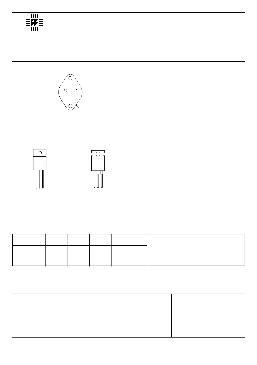
Pin 1 ≠ Ground
Pin 2 ≠ V
OUT
Case ≠ V
IN
K Package ≠ TO≠3
Pin 1 ≠ Ground
Pin 2 ≠ V
IN
Pin 3 ≠ V
OUT
Case ≠ V
IN
T Package ≠ TO≠220
1
2
3
1
2
3
Order Information
Part K≠Pack
G≠Pack
T≠Pack
Temp.
Number
(TO≠3)
(TO≠257) (TO≠220)
Range
IP1R17Axx≠zz
-55 to +150∞C
IP1R17xx≠zz
"
IP3R17Azz≠xx
0 to +125∞C
IP3R17zz≠xx
"
Note:
xx = Voltage Code
(05, 12, 15)
eg.
IP1R17AK≠05
zz = Package Code
(G, K, T)
IP3R17G≠12
Pin 1 ≠ Ground
Pin 2 ≠ V
IN
Pin 3 ≠ V
OUT
Case ≠ V
IN
G Package ≠ TO≠257
1 2 3

LAB
SEME
IP1R17A
IP3R17A
IP1R17
A
IP3R17
A
Semelab plc.
Telephone (01455) 556565. Telex: 341927. Fax (01455) 552612.
Prelim. 4/96
IP1R17A≠05
IP1R17≠05
IP3R17A≠05
IP3R17≠05
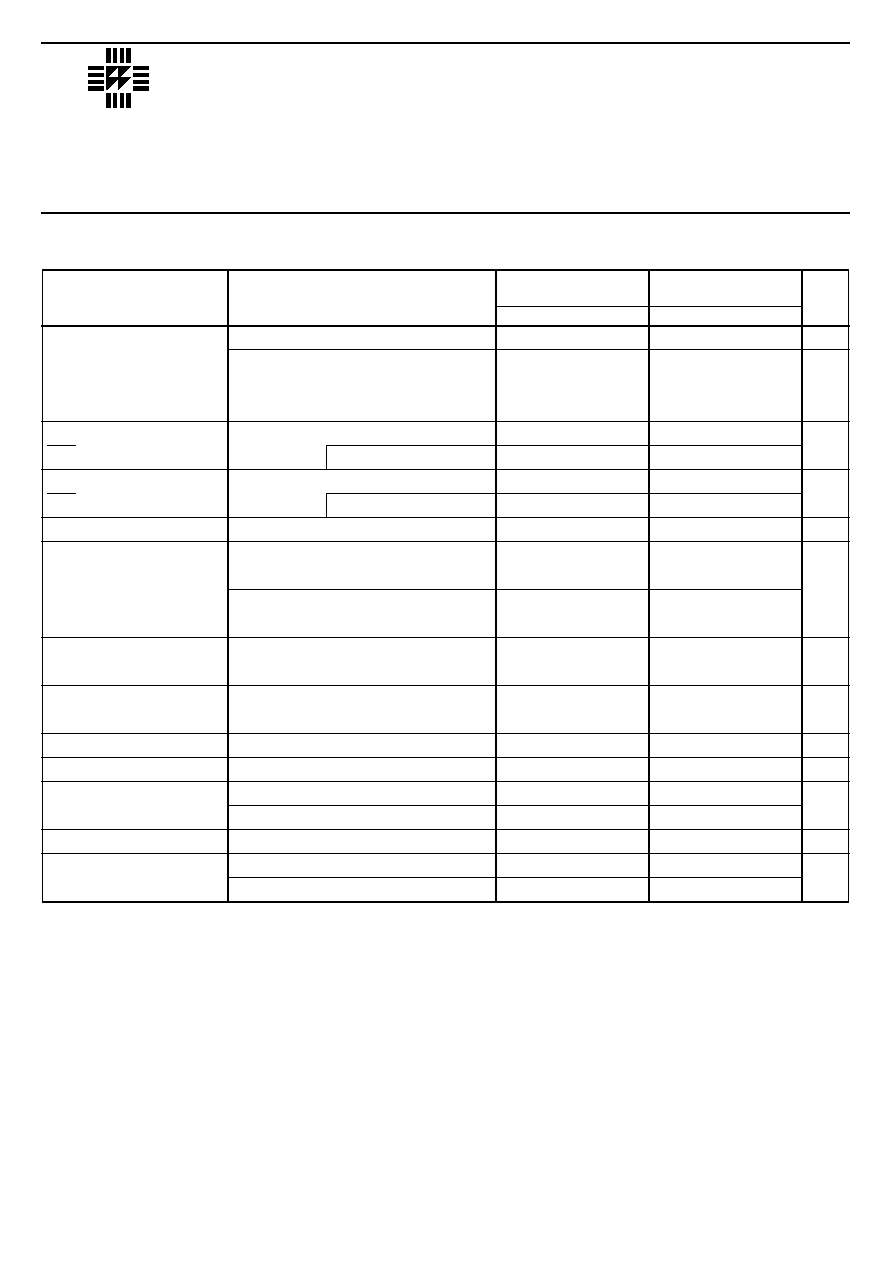
Parameter
Test Conditions
2
Min.
Typ.
Max.
Min.
Typ.
Max. Units
V
O
V
O
V
I
V
O
I
O
I
Q
I
Q
V
D
I
PEAK
I
SC
e
n
R
JC
Output Voltage
Line Regulation
Load Regulation
Quiescent Current
Quiescent Current
Change
Dropout Voltage
Ripple Rejection
Thermal Regulation
Peak Output Current
Short Circuit Current
Output Noise Voltage
Thermal Resistance
Junction to Case
I
O
= -5mA to -3A
P
P
MAX
V
IN
= -8V to -20V
T
J
= Over Temp. Range
1
V
IN
= -7.5V to -35V
I
O
= -5mA
3
T
J
= Over Temp. Range
1
I
O
= -5mA to -3A
3
T
J
= Over Temp. Range
1
I
O
= -5mA
T
J
= Over Temp. Range
1
I
O
= -5mA to -3A
T
J
= Over Temp. Range
1
I
O
= -5mA
V
IN
= -7.5V to -35V
T
J
= Over Temp. Range
1
I
O
= -3A
V
OUT
= 100mV
T
J
= Over Temp. Range
1
I
O
= -1A
f = 120Hz
T
J
= Over Temp. Range
1
t
p
= 20ms
P = P
MAX
V
IN
= -10V
T
J
= Over Temp. Range
1
V
IN
= -10V
V
IN
= -35V
f = 10Hz to 100kHz
K Package
G, T Package
-5.15
-5
-4.85
-5.25
-4.75
6
30
12
60
10
50
20
100
5
10
5
2.2
3
60
80
0.002
0.02
-6.5
-4.5
-4
-1
40
1.5
2.5
3
4
-5.05
-5
-4.95
-5.15
-4.85
3
15
6
30
5
25
10
50
5
10
5
2.2
3
60
80
0.002
0.01
-6.5
-4.5
-4
-1
40
1.5
2.5
3
4
V
V
mV
mV
mA
mA
V
dB
%/W
A
A
µ
V
∞C/W
ELECTRICAL CHARACTERISTICS
(T
C
= 25∞C unless otherwise stated)
Notes
1) Applies over full temperature range:≠
T
J
= ≠55 to +150∞C for IP1R17A≠05 / IP1R17≠05
T
J
=
0 to +125∞C for IP3R17A≠05 / IP3R17≠05
All other specifications apply at T
C
= 25∞C unless otherwise stated.
2) Test conditions unless otherwise stated:≠
V
IN
= -10V , I
OUT
= -1.5A .
Although Power Dissipation is internally limited, these specifications apply for Power Dissipation up to 30W for the TO≠3
Package, and 20W for the TO≠220 and TO≠257 Packages.
3) Load and Line regulation are electrically independent and are measured using pulse techniques at low duty cycle in order to
maintain constant junction temperature. To determine the effects on the output voltage due to device heating, refer to thermal
regulation specification.
LAB
SEME
IP1R17A
IP3R17A
IP1R17
A
IP3R17
A
Semelab plc.
Telephone (01455) 556565. Telex: 341927. Fax (01455) 552612.
Prelim. 4/96
IP1R17A≠12
IP1R17≠12
IP3R17A≠12
IP3R17≠12
Parameter
Test Conditions
2
Min.
Typ.
Max.
Min.
Typ.
Max.
Units
V
O
V
O
V
I
V
O
I
O
I
Q
I
Q
V
D
I
PEAK
I
SC
e
n
R
JC
Output Voltage
Line Regulation
Load Regulation
Quiescent Current
Quiescent Current
Change
Dropout Voltage
Ripple Rejection
Thermal Regulation
Peak Output Current
Short Circuit Current
Output Noise Voltage
Thermal Resistance
Junction to Case
I
O
= -5mA to -3A
P
P
MAX
V
IN
= -15V to -27V
T
J
= Over Temp. Range
1
V
IN
= -14.5V to -35V
I
O
= -5mA
3
T
J
= Over Temp. Range
1
I
O
= -5mA to -3A
3
T
J
= Over Temp. Range
1
I
O
= -5mA
T
J
= Over Temp. Range
1
I
O
= -5mA to -3A
T
J
= Over Temp. Range
1
I
O
= -5mA
V
IN
= -14.5V to -35V
T
J
= Over Temp. Range
1
I
O
= -3A
V
OUT
= 250mV
T
J
= Over Temp. Range
1
I
O
= -1A
f = 120Hz
T
J
= Over Temp. Range
1
t
p
= 20ms
P = P
MAX
V
IN
= -17V
T
J
= Over Temp. Range
1
V
IN
= -17V
V
IN
= -35V
f = 10Hz to 100kHz
K Package
G, T Package
-12.36
-12
-11.64
-12.60
-11.40
10
60
20
120
20
120
40
240
5
10
5
2.2
3
52
72
0.002
0.02
-6.5
-4.5
-2.5
-1
75
1.5
2.5
3
4
-12.12
-12
-11.88
-12.36
-11.64
5
30
10
60
10
60
20
120
5
10
5
2.2
3
52
72
0.002
0.01
-6.5
-4.5
-2.5
-1
75
1.5
2.5
3
4
V
V
mV
mV
mA
mA
V
dB
%/W
A
A
µ
V
∞C/W
ELECTRICAL CHARACTERISTICS
(T
J
= 25∞C unless otherwise stated)
Notes
1) Applies over full temperature range:≠
T
J
= ≠55 to +150∞C for IP1R17A≠12 / IP1R17≠12
T
J
=
0 to +125∞C for IP3R17A≠12 / IP3R17≠12
All other specifications apply at T
C
= 25∞C unless otherwise stated.
2) Test conditions unless otherwise stated:≠
V
IN
= -17V , I
OUT
= -1.5A .
Although Power Dissipation is internally limited, these specifications apply for Power Dissipation up to 30W for the TO≠3
Package, and 20W for the TO≠220 and TO≠257 Packages.
3) Load and Line regulation are electrically independent and are measured using pulse techniques at low duty cycle in order to
maintain constant junction temperature. To determine the effects on the output voltage due to device heating, refer to thermal
regulation specification.

LAB
SEME
IP1R17A
IP3R17A
IP1R17
A
IP3R17
A
Semelab plc.
Telephone (01455) 556565. Telex: 341927. Fax (01455) 552612.
Prelim. 4/96
IP1R17A≠15
IP1R17≠15
IP3R17A≠15
IP3R17≠15
Parameter
Test Conditions
2
Min.
Typ.
Max.
Min.
Typ.
Max. Units
V
O
V
O
V
I
V
O
I
O
I
Q
I
Q
V
D
I
PEAK
I
SC
e
n
R
JC
Output Voltage
Line Regulation
Load Regulation
Quiescent Current
Quiescent Current
Change
Dropout Voltage
Ripple Rejection
Thermal Regulation
Peak Output Current
Short Circuit Current
Output Noise Voltage
Thermal Resistance
Junction to Case
I
O
= -5mA to -3A
P
OUT
P
MAX
V
IN
= -18V to -30V
T
J
= Over Temp. Range
1
V
IN
= -17.5V to -35V
I
O
= -5mA
3
T
J
= Over Temp. Range
1
I
O
= -5mA to -3A
3
T
J
= Over Temp. Range
1
I
O
= -5mA
T
J
= Over Temp. Range
1
I
O
= -5mA to -3A
T
J
= Over Temp. Range
1
I
O
= -5mA
V
IN
= -17.5V to -35V
T
J
= Over Temp. Range
1
I
O
= -3A
V
OUT
= 300mV
T
J
= Over Temp. Range
1
I
O
= -1A
f = 120Hz
T
J
= Over Temp. Range
1
t
p
= 20ms
P = P
MAX
V
IN
= -20V
T
J
= Over Temp. Range
1
V
IN
= -20V
V
IN
= -35V
f = 10Hz to 100kHz
K Package
G, T Package
-15.45
-15
-14.55
-15.75
-14.25
16
80
32
160
32
160
64
320
5
10
5
2.2
3
50
70
0.002
0.02
-6.5
-4.5
-2.3
-1
90
1.5
2.5
3
4
-15.15
-15
-14.85
-15.45
-14.55
8
40
16
80
16
80
32
160
5
10
5
2.2
3
50
70
0.002
0.01
-6.5
-4.5
-2.3
-1
90
1.5
2.5
3
4
V
V
mV
mV
mA
mA
V
dB
%/W
A
A
µ
V
∞C/W
ELECTRICAL CHARACTERISTICS
(T
J
= 25∞C unless otherwise stated)
Notes
1) Applies over full temperature range:≠
T
J
= ≠55 to +150∞C for IP1R17A≠15 / IP1R17≠15
T
J
=
0 to +125∞C for IP3R17A≠15 / IP3R17≠15
All other specifications apply at T
C
= 25∞C unless otherwise stated.
2) Test conditions unless otherwise stated:≠
V
IN
= -20V , I
OUT
= -1.5A .
Although Power Dissipation is internally limited, these specifications apply for Power Dissipation up to 30W for the TO≠3
Package, and 20W for the TO≠220 and TO≠257 Packages.
3) Load and Line regulation are electrically independent and are measured using pulse techniques at low duty cycle in order to
maintain constant junction temperature. To determine the effects on the output voltage due to device heating, refer to thermal
regulation specification.