 | –≠–ª–µ–∫—Ç—Ä–æ–Ω–Ω—ã–π –∫–æ–º–ø–æ–Ω–µ–Ω—Ç: IP2524B | –°–∫–∞—á–∞—Ç—å:  PDF PDF  ZIP ZIP |
LAB
SEME
IP1524B SERIES
Semelab plc.
Telephone (01455) 556565. Telex: 341927. Fax (01455) 552612.
Prelim. 3/95
REGULATING
PULSE WIDTH
MODULATORS
FEATURES
∑ Pin Compatible with IP1524 Series
∑ 7 to 40 volt operation
∑ 5 volt reference trimmed to ±1%
∑ Undervoltage lockout
∑ Excellent external sync capability
∑ Wide current limit common mode range
∑ +5 Volt error amplifier common mode
∑ PWM data latch
∑ Full double-pulse suppression logic
∑ 50ns shutdown function
∑ Dual 200mA, 60V output transistors
∑ Fully specified over temperature
+V
IN
Input Voltage
Collector Voltage
Logic Inputs
Current Limit Sense Inputs
Oscillator Charging Current
P
D
Power Dissipation
T
A
= 25∞C
Derate @ T
A
> 50∞C
P
D
Power Dissipation
T
C
= 25∞C
Derate @ T
C
> 25∞C
T
J
Operating Junction Temperature
T
STG
Storage Temperature Range
T
L
Lead Temperature
(soldering, 10 seconds)
+40V
+60V
≠0.3 to +5.5V
≠0.3 to +V
IN
5mA
1W
10mW/∞C
2W
16mW/∞C
See Ordering Information
≠65 to +150∞C
+300∞C
ABSOLUTE MAXIMUM RATINGS
(T
case
= 25∞C unless otherwise stated)
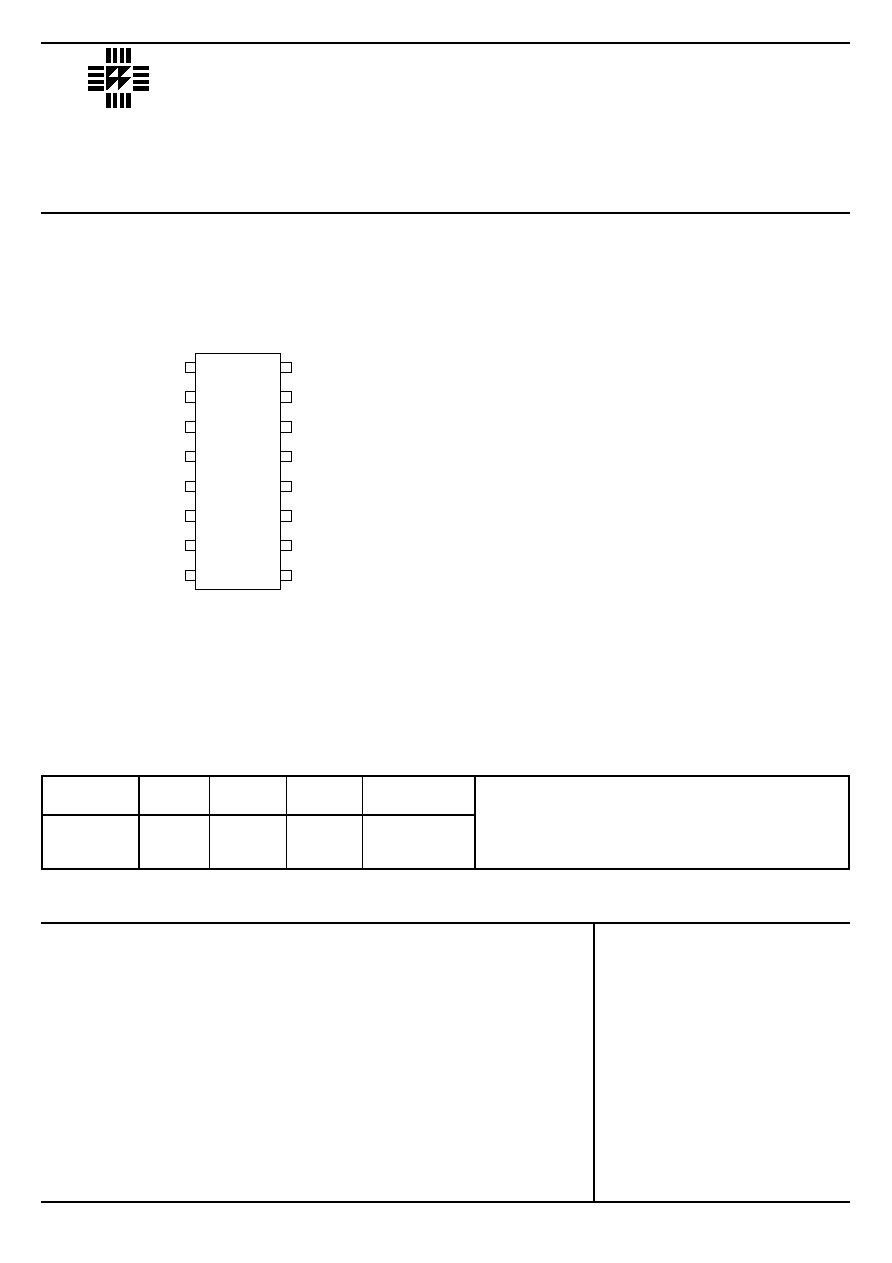
TOP VIEW
J Package ≠ 16 Pin Ceramic DIP
N Package ≠ 16 Pin Plastic DIP
D Package ≠ 16 Pin Plastic (300) SOIC
8
1
2
3
4
5
6
7
14
13
12
11
10
9
15
16
INV. INPUT
N. I. INPUT
OSC. OUTPUT
+C.L. SENSE
≠C.L. SENSE
R
T
C
T
GROUND
V
REF
V
IN
E
B
C
B
C
A
E
A
SHUTDOWN
COMPENSATION
Part J≠Pack
N≠Pack
D≠16
Temp.
Number
16 Pin
16 Pin
16 Pin
Range
IP1524B
-55 to +125∞C
IP2524B
-25 to +85∞C
IP3524B
0 to +70∞C
Order Information
Note:
To order, add the package identifier to the part number.
eg.
IP1524BJ
IP3524BD≠16
LAB
SEME
IP1524B SERIES
Semelab plc.
Telephone (01455) 556565. Telex: 341927. Fax (01455) 552612.
Prelim. 3/95
E
C
C.L.
+C.L.
SENSE
≠C.L.
SENSE
INV.
INPUT
N.I.
INPUT
T
T
6
7
OSCILLATOR
R
C
15
8
REFERENCE
REGULATOR
GND
UNDER
VOLTAGE
LOCKOUT
TO INTERNAL
CIRCUITRY
OSC.
D
S Q
Q
S
Q
R
Q
T
Q
1
2
5
4
COMPENSATION
SHUTDOWN
9
10
PWM
LATCH
MEMORY
F/F
TOGGLE
F/F
PWM
ERROR
+V
IN
V
REF
16
3
C
E
B
B
A
A
11
12
13
14
+7 to +40V
0 to +60V
+2.3 to V
REF
0 to V
IN
≠ 2.5V
0 to 200mA
0 to 20mA
25
µ
A to 1.8mA
50Hz to 500kHz
2k
to 150k
1nF to 0.1
µ
F
≠55 to +125∞C
≠25 to +85∞C
0 to +70∞C
RECOMMENDED OPERATING CONDITIONS
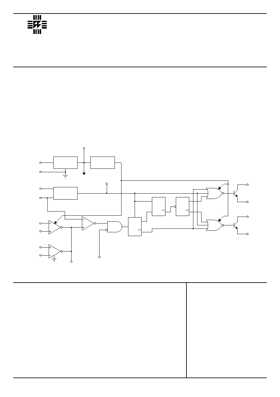
DESCRIPTION
The IP1524B is a pulse width modulator for switching power supplies which features improved performance over
industry standards like the SG1524. A direct pin-for-pin replacement for the earlier device, it combines advanced
processing techniques and circuit design to provide improved reference accuracy/ and extended common mode range at
the error amplifier and current limit inputs. A DC-coupled flip-flop eliminates triggering and glitch problems, and a PWM
data latch prevents edge oscillations. The circuit incorporates true digital shutdown for high speed response, while an
undervoltage lockout circuit prevents spurious outputs when the supply voltage is too low for stable operation. Full
double-pulse suppression logic insures alternating output pulses when the shutdown pin is used for pulse-by-pulse
current limiting.
BLOCK DIAGRAM
V
IN
Input Voltage
Collector Voltage
Error Amp Common Mode Range
Current Limit Sense Common Mode Range
Output Current
(each transistor)
Reference Load Current
Oscillator Charging Current
Oscillator Frequency Range
R
T
Oscillator Timing Resistor
C
T
Oscillator Timing Capacitor
Operating Ambient Temperature Range
IP1524B
IP2524B
IP3524B
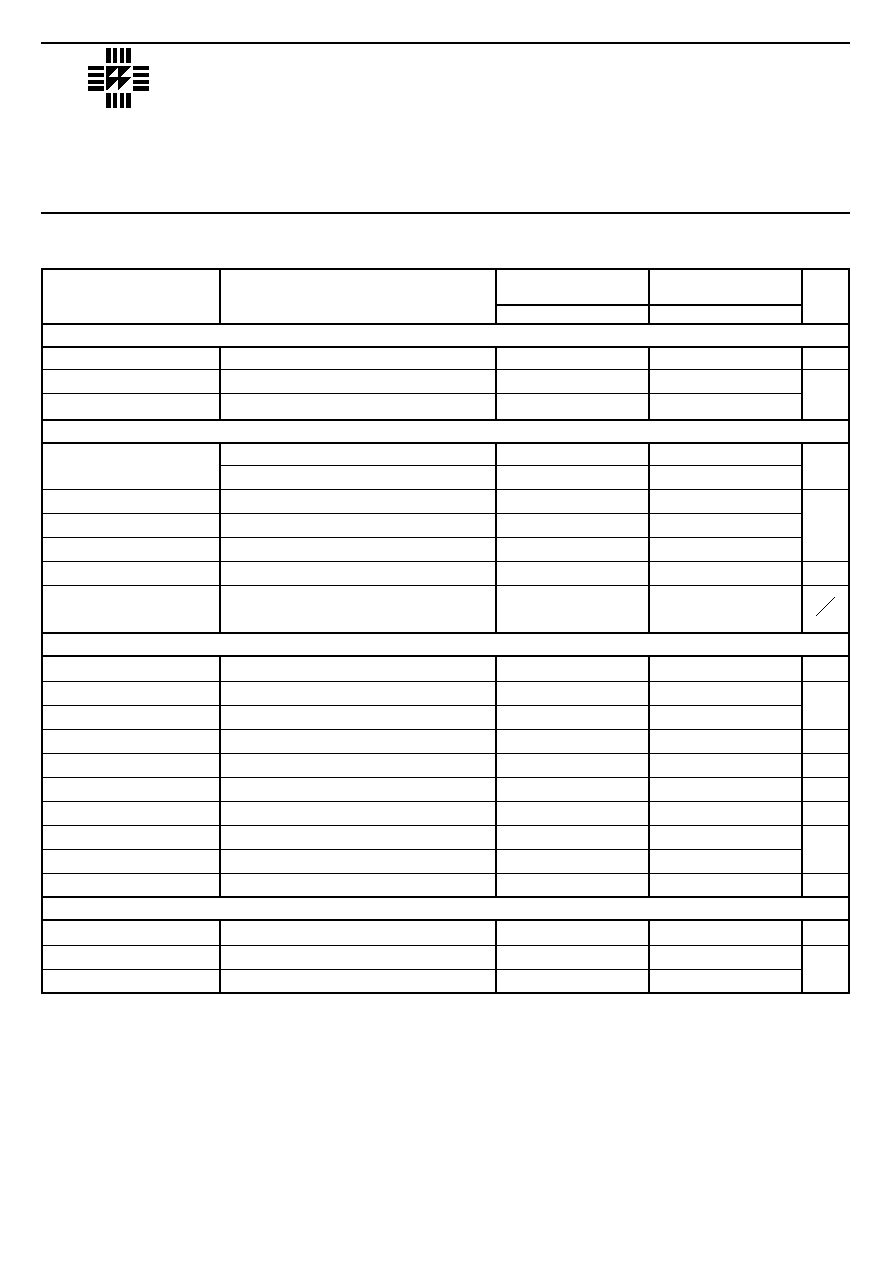
NOTES
1. Test Conditions unless otherwise stated:
V
IN
= 20V , I
REF
= 0.
T
J
= ≠55 to +125∞C for IP1524B
T
J
= ≠25 to +85∞C
for IP2524B
T
J
= 0 to +70∞C
for IP3524B
2. R
T
= 2.7K
, C
T
= 0.01
µ
F unless otherwise stated.
LAB
SEME
IP1524B SERIES
Semelab plc.
Telephone (01455) 556565. Telex: 341927. Fax (01455) 552612.
Prelim. 3/95
4.3
5.2
6.5
0.1
0.3
0.6
7
10
4.90
5.00
5.10
4.85
5.15
1
15
5
25
40
75
25
70
120
1
39
43
47
0.1
1
1
2
80
140
400
700
3.0
4.0
0.4
0.5
1.2
3.7
4.0
0.6
1
1.1
-1
2
10
1
10
0.1
1
4.3
5.2
6.5
0.1
0.3
0.6
7
10
4.95
5.00
5.05
4.90
5.10
1
10
5
15
40
75
25
70
120
1
10
41
43
45
0.1
1
1
2
80
140
400
700
3.0
4.0
0.4
0.5
1.2
3.7
4.0
0.6
1
1.1
-1
0.1
5
1
5
0.1
1
IP1524B
IP2524B
IP3524B
Parameter
Test Conditions
1
Min.
Typ.
Max.
Min.
Typ.
Max.
Units
V
IN
Undervoltage Threshold
Turn≠on Hysteresis
Operating Current
Output Voltage
Line Regulation
Load Regulation
Temperature Stability
Short Circuit Current
Long Term Stability
Initial Accuracy
Voltage Stability
Temperature Stability
Minimum Frequency
Maximum Frequency
Clock Amplitude
Clock Pulse Width
Sawtooth Peak Voltage
Sawtooth Valley Voltage
Sawtooth Valley T.C.
Input Offset Voltage
Input Bias Current
Input Offset Current
V
IN
Rising
V
IN
= 7 to 40V
T
J
= 25∞C
V
IN
= 7 to 40V
I
L
= 0 to 20mA
V
IN
= 7 to 40V
I
L
= 0 to 20mA
V
REF
= 0
T
J
= 25∞C
T
J
= 25∞C
V
IN
= 7 to 40V
R
T
= 150k
C
T
= 0.1
µ
F
R
T
= 2k
C
T
= 470pF
Output, Pin 3
C
T
= 0.01
µ
F
Output, Pin 3
C
T
= 0.01
µ
F
C
T
= 0.01
µ
F
C
T
= 0.01
µ
F
T
J
= 25∞C
V
CM
= 2.3 to V
REF
V
CM
= 2.3 to V
REF
V
CM
= 2.3 to V
REF
V
mA
V
mV
mA
mV
khr
kHz
%
Hz
kHz
V
µ
s
V
mV/∞C
mV
µ
A
ELECTRICAL CHARACTERISTICS
(T
J
= Over Operating Temperature Range unless otherwise stated)
ERROR AMP SECTION
OSCILLATOR SECTION
2
REFERENCE SECTION
TURN≠ON CHARACTERISTICS
IP1524B
IP2524B
IP3524B
Parameter
Test Conditions
1
Min.
Typ.
Max.
Min.
Typ.
Max.
Units
60
75
70
90
76
120
0.2
0.5
3.8
4.2
1
2
0
45
49
180
200
220
-1
-10
2.0
0.1
1
0.6
50
0.1
20
0.2
0.4
1.0
2.2
17
19
16.5
18
0.2
0.1
60
75
70
90
76
120
0.2
0.5
3.8
4.2
1
2
0
45
49
180
200
220
-1
-10
2.0
0.1
1
0.6
50
0.1
20
0.2
0.4
1.0
2.2
17
19
16.5
18
0.2
0.4
0.1
0.2
DC Open Loop Gain
Common Mode Rejection
Supply Voltage Rejection
Output Low Level
Output High Level
Gain Bandwidth Product
Minimum Duty Cycle
Maximum Duty Cycle
Sense Voltage
Input Bias Current
High Input Voltage
High Input Current
Low Input Voltage
Shutdown Delay
Collector Leakage Current
Collector Saturation Voltage
Emitter Output Voltage
Emitter Voltage Rise Time
Collector Voltage Fall Time
V
O
= 1 to 3V
R
L
10M
V
CM
= 2.3 to V
REF
V
IN
= 7 to 40V
I
SINK
= 100
µ
A
I
SOURCE
= 100
µ
A
T
J
= 25∞C
V
PIN1
≠ V
PIN2
150mV
V
PIN2
≠ V
PIN1
150mV
V
CM
= 0 to 17.5V
V
IN
= 7 to 40V
V
CM
= 0 to 17.5V
V
IN
= 7 to 40V
V
SHUTDOWN
= 5V
Pin 10 to output
T
J
= 25∞C
V
CE
= 60V
I
C
= 20mA
I
C
= 200mA
I
E
= 50mA
I
E
= 200mA
R
E
= 2k
T
J
= 25∞C
R
C
= 2k
T
J
= 25∞C
dB
V
MHz
%
mV
µ
A
V
mA
V
ns
µ
A
V
V
µ
s
LAB
SEME
IP1524B SERIES
Semelab plc.
Telephone (01455) 556565. Telex: 341927. Fax (01455) 552612.
Prelim. 3/95
PWM COMPARATOR
ERROR AMP SECTION (cont.)
CURRENT LIMIT AMPLIFIER
SHUTDOWN INPUT
OUTPUT SECTION (each transistor)
NOTES
1. Test Conditions unless otherwise stated:
V
IN
= 20V , I
REF
= 0.
T
J
= ≠55 to +125∞C for IP1524B
T
J
= ≠25 to +85∞C
for IP2524B
T
J
= 0 to +70∞C
for IP3524B
ELECTRICAL CHARACTERISTICS
(T
J
= Over Operating Temperature Range unless otherwise stated)
LAB
SEME
IP1524B SERIES
Semelab plc.
Telephone (01455) 556565. Telex: 341927. Fax (01455) 552612.
Prelim. 3/95
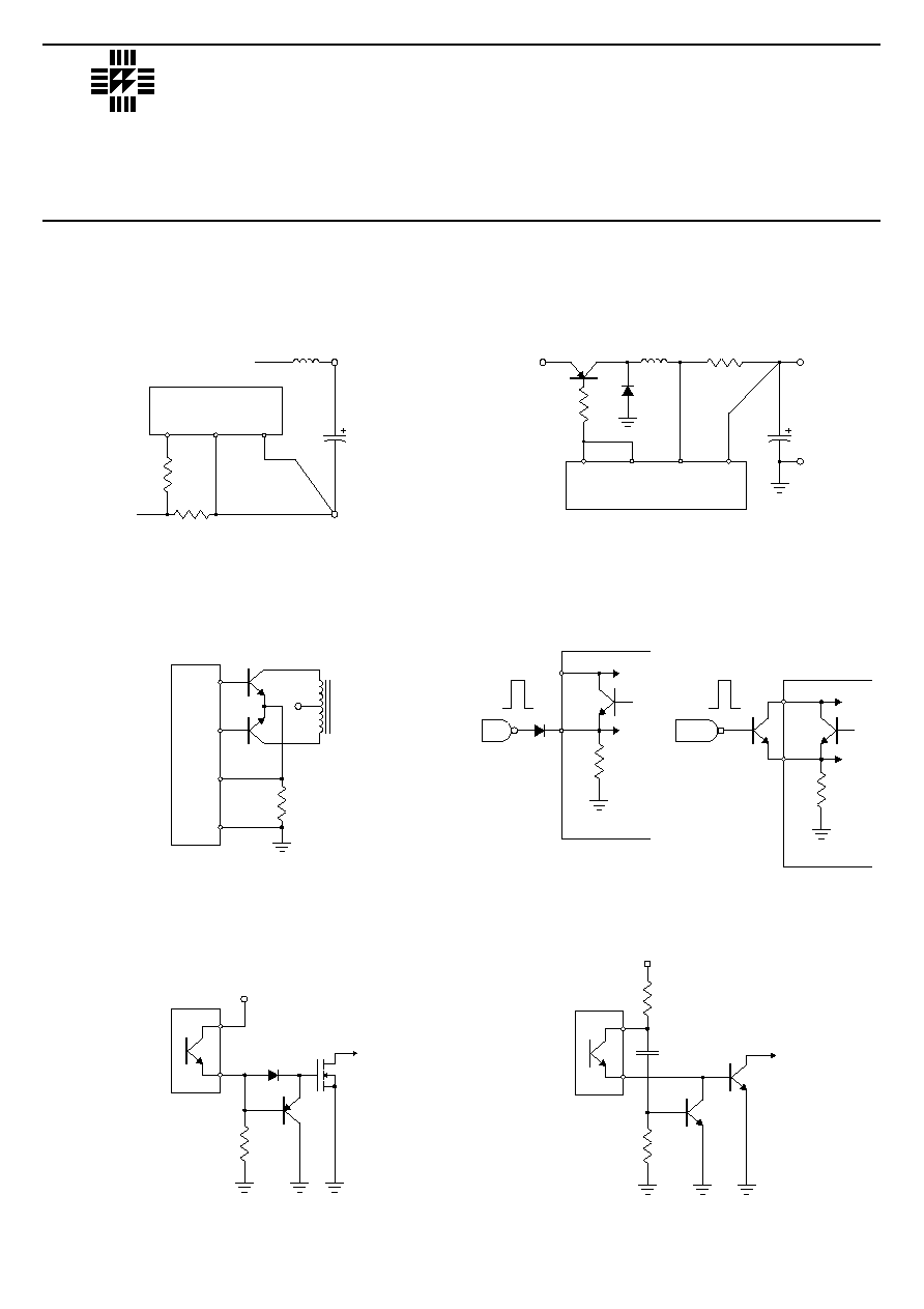
APPLICATIONS INFORMATION
8
5
4
OUT
SENSE
+C.L.
≠C.L.
GND
100
RAW
SUPPLY
RETURN
RETURN
+V
R
SENSE
OUT
+C.L.
≠C.L.
RETURN
RAW
SUPPLY
C
C
R
+V
13
5
4
12
A
B
11
+C.L.
≠C.L.
E
B
E
A
14
4
5
SENSE
R
3
16
3.2k
TTL
3
16
3.2k
CMOS
1N914
2N2369
11
12
+15V
D1
Q1
1.6k
TO
LOAD
11
12
Q1
4.7k
1.6k
0.01
µ
F
Q2
TO
LOAD
Current Sensing in the Ground Line
Sensing Primary Current
with an Emitter Resistor
Driving Power MOSFETs
Current Sensing in the Output Line
Oscillator Sync to an External Clock
A. TTL Logic
B. 5 Volt CMOS Logic
Driving Power Bipolar Transistors