LAB
SEME
IP1524 SERIES
Semelab plc.
Telephone (01455) 556565. Telex: 341927. Fax (01455) 552612.
Prelim. 3/95
REGULATING
PULSE WIDTH
MODULATORS
FEATURES
∑ Guaranteed ±2% reference voltage tolerance
∑ Guaranteed ±6% oscillator tolerance
∑ Fully specified temperature performance
∑ Guaranteed 10mV/1000 hours long term stability
∑ Interchangeable with SG1524 series
+V
IN
Input Voltage
Collector Voltage
Output Current
(each transistor)
Reference Load Current
Oscillator Charging Current
Shut Down Pin Voltage
Current Limit Sense Common Mode Range
P
D
Power Dissipation
T
A
= 25∞C
Derate @ T
A
> 50∞C
P
D
Power Dissipation
T
C
= 25∞C
Derate @ T
C
> 25∞C
T
J
Operating Junction Temperature
T
STG
Storage Temperature Range
T
L
Lead Temperature
(soldering, 10 seconds)
+40V
+40V
100mA
Internally Limited
5mA
+5.5V
≠1.0 to +1.0V
1W
10mW/∞C
2W
16mW/∞C
See Ordering Information
≠65 to +150∞C
+300∞C
ABSOLUTE MAXIMUM RATINGS
(T
case
= 25∞C unless otherwise stated)
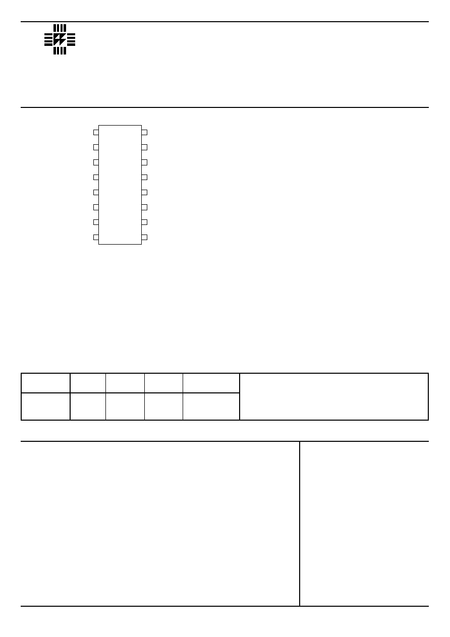
TOP VIEW
J Package ≠ 16 Pin Ceramic DIP
N Package ≠ 16 Pin Plastic DIP
D Package ≠ 16 Pin Plastic (150) SOIC
8
1
2
3
4
5
6
7
14
13
12
11
10
9
15
16
INV. INPUT
N. I. INPUT
OSC. OUTPUT
+C.L. SENSE
≠C.L. SENSE
R
T
C
T
GROUND
V
REF
V
IN
E
B
C
B
C
A
E
A
SHUTDOWN
COMPENSATION
Part J≠Pack
N≠Pack
D≠16
Temp.
Number
16 Pin
16 Pin
16 Pin
Range
IP1524
-55 to +125∞C
IP2524
-25 to +85∞C
IP3524
0 to +70∞C
Order Information
Note:
To order, add the package identifier to the part number.
eg.
IP1524J
IP3524D≠16
LAB
SEME
IP1524 SERIES
Semelab plc.
Telephone (01455) 556565. Telex: 341927. Fax (01455) 552612.
Prelim. 3/95
V
R
C
+5V TO ALL
INTERNAL CIRCUITRY
INV.
INPUT
ERROR
AMP
REFERENCE
REGULATOR
OSCILLATOR
OSCILLATOR
OUTPUT
FLIP
FLOP
COMPARATOR
+5V
NOR
NOR
SHUTDOWN
C
E
C
E
+5V
C.L.
N.I.
INPUT
GND
(SUBSTRATE)
COMPENSATION
+SENSE
≠SENSE
+5V
4
9
5
1
2
8
10
IN
T
T
15
6
7
A
A
B
B
12
11
13
14
16
3
1k
10k
+8 to +40V
0 to +40V
+1.8 to +3.4V
0 to 100mA
0 to 20mA
30
µ
A to 2mA
50Hz to 500kHz
1.8k
to 100k
1nF to 0.1
µ
F
≠55 to +125∞C
-25 to +85∞C
0 to +70∞C
RECOMMENDED OPERATING CONDITIONS
DESCRIPTION
The IP1524 series of PWM switching regulator control circuits contains all the functions required to implement single-
ended or push-pull switching regulators. Included are voltage reference, error amplifer, oscillator, PWM comparator,
output drivers, current limiting and shutdown circuitry.
Although functionally indentical to the SG1524 series, SEMELAB has incorporated several improvements to the IP1524
allowing tighter and more complete specification of electrical performance.
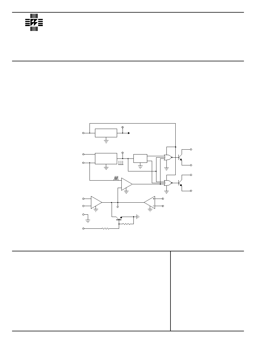
BLOCK DIAGRAM
V
IN
Input Voltage
Collector Voltage
Error Amp Common Mode Range
Output Current
(each transistor)
Reference Load Current
Oscillator Charging Current
Oscillator Frequency Range
R
T
Oscillator Timing Resistor
C
T
Oscillator Timing Capacitor
T
AMB
Operating Ambient Temperature Range
IP1524
IP2524
IP3524
NOTES
1. Test Conditions unless otherwise stated: V
IN
= 20V , I
REF
= 0.
2. V
CM
= +1.8 to +3.4V
3. V
CM
= -1 to +1V
IP1524
IP2524
IP3524
Parameter
Test Conditions
1
Min.
Typ.
Max.
Min.
Typ.
Max.
Units
0
45
49
180
200
220
200
1.2
4
0.3
40
0.1
50
1
2
17
18
0.2
0.1
5
10
0
45
49
190
200
210
170
200
230
1.2
4
8
0.3
40
0.1
50
1
2
17
18
0.2
0.4
0.1
0.2
5
10
Minimum Duty Cycle
Maximum Duty Cycle
Sense Voltage
High Input Voltage
High Input Current
Low Input Voltage
Collector ≠ Emitter Voltage
Collector Leakage Current
Collector Saturation
Voltage
Emitter Output Voltage
Emitter Voltage Rise Time
Collector Voltage Fall Time
Standby Current
V
PIN1
≠ V
PIN2
150mV
T
J
= Over Temp. Range
V
PIN2
≠ V
PIN1
150mV
T
J
= Over Temp. Range
V
CM
= 0
V
CM
= 0
T
J
= Over Temp. Range
V
PIN9
0.6V
T
J
= Over Temp. Range
V
SHUTDOWN
= +5V
T
J
= Over Temp. Range
V
PIN9
3.5V
T
J
= Over Temp. Range
I
C
= 50
µ
A
T
J
= Over Temp. Range
V
CE
= 40V
T
J
= Over Temp. Range
I
C
= 50mA
T
J
= Over Temp. Range
V
IN
= 20V
T
J
= Over Temp. Range
R
E
= 2k
R
C
= 2k
V
IN
= 40V
T
J
= Over Temp. Range
%
%
mV
V
mA
V
V
µ
A
V
V
µ
s
mA
LAB
SEME
IP1524 SERIES
Semelab plc.
Telephone (01455) 556565. Telex: 341927. Fax (01455) 552612.
Prelim. 3/95
ELECTRICAL CHARACTERISTICS
(T
J
= 25∞C unless otherwise stated)
PWM COMPARATOR
POWER CONSUMPTION
CURRENT LIMIT AMPLIFIER
3
SHUTDOWN INPUT
OUTPUT SECTION (each transistor)
LAB
SEME
IP1524 SERIES
Semelab plc.
Telephone (01455) 556565. Telex: 341927. Fax (01455) 552612.
Prelim. 3/95
APPLICATIONS INFORMATION
The IP1524 is a fixed-frequency pulse-width
modulation voltage regulator control circuit. The
regulator operates at a frequency that is programmed
by one timing resistor (R
T
) and one timing capacitor
(C
T
). R
T
establishes a constant charging current for C
T
,
which is fed to the comparator providing linear control of
the output pulse width by the error amplifier.
The IP1524 contains an on-board 5V regulator that
serves as a reference as well as powering the IP1524's
internal control circuitry and is also useful in supplying
external support functions. This reference voltage is
lowered externally by a resistor divider to provide a
reference within the common-mode range of the error
amplifier or an external reference may be used. The
power supply output is sensed by a second resistor
divider network to generate a feedback signal to the
error amplifier. The amplifier output voltage is then
compared to the linear voltage ramp at C
T
. The
resulting modulated pulse out of the high-gain
comparator is then steered to the appropriate output
pass transistor (Q
1
or Q
2
) by the pulse-steering flip-flop,
which is synchronously toggled by the oscillator output.
The oscillator output pulse also serves as a blanking
pulse to assure both outputs are never on
simultaneously during the transition times.
The width of the blanking pulse is controlled by the
value of C
T
.
The outputs may be applied in a push-pull
configuration in which their frequency is half that of the
base oscillator, or paralleled for single-ended
applications in which the frequency is equal to that of
the oscillator. The output of the error amplifier shares a
common input to the comparator with the current
limiting and shutdown circuitry and can be overridden
by signals from either of these inputs.
This common point is also available externally and
may be employed to control the gain of, or to
compensate, the error amplifier, or to provide additional
control to the regulator.
RE F
V
R
T
C
T
I NV .
N. I.
O S C .
S H . D O W N
C O M P .
C
A
E
A
E
B
C
B
C +
L
C -
L
I N
V
G N D
+ 2 8 V
R E T U R N
G N D
+ 5 V
1 A
0 . 1
µ
F
0 . 0 2
µ
F
0 . 1
5 0 0
µ
F
1 N3 8 8 0
5 k
5 k
5 k
5 k
3 k
0 .0 0 1
µ
F
6 8
1 5 0
2 k
5 0 k
0 .9 m H
RE F
V
R
T
C
T
I N V .
N. I.
O S C .
S H . D O W N
C O M P .
C
A
E
A
E
B
C
B
C +
L
C -
L
I N
V
G N D
+ 2 8 V
R E T U R N
0 .1
µ
F
0 . 0 1
µ
F
5 k
5 k
5 k
5 k
0 .0 0 1
µ
F
1 m H
2 k
2 0 k
1 k
1 W
1 k
1 W
1 k
1 k
2 0
T
2 0
T
1 0 0
µ
F
0 . 1
5
T
5
T
5 V
5 A
1 0 0
µ
F
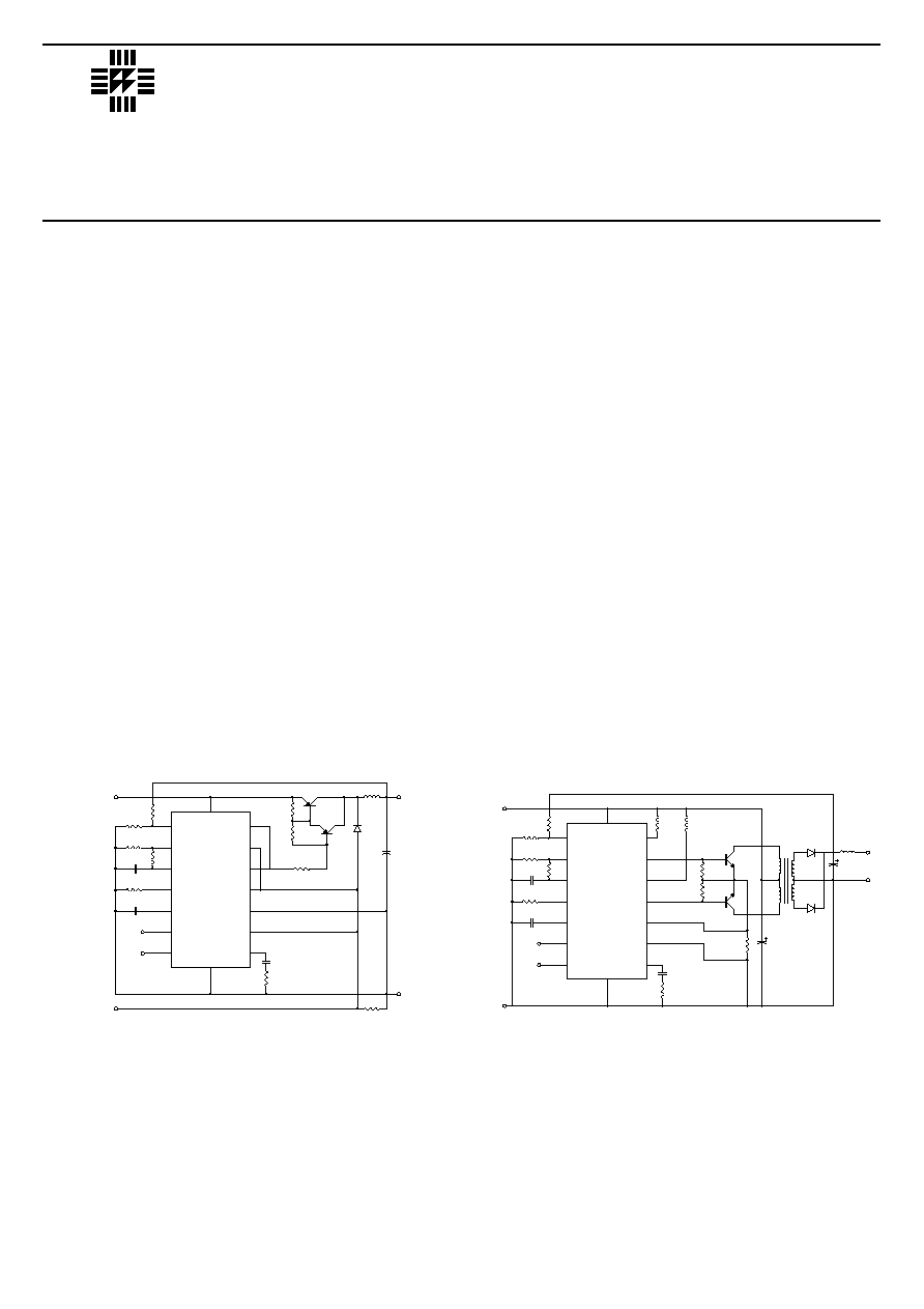
In this conventional single-ended regulator circuit, the two outputs of
the IP1524 are connected in parallel for effective 0-90% duty cycle
modulation. The use of an output inductor requires an R-C phase
compensation network for loop stability.
Push-pull outputs are used in this transformer-coupled DC-DC
regulating converter. Note that the oscillator must be set at twice the
desired output frequency as the IP1524's internal flip-flop divides the
frequency by 2 as it switches the PWM signal from one output to the
other. Current limiting is done in the primary so that the pulse width will
be reduced should transformer saturation occur.