 | –≠–ª–µ–∫—Ç—Ä–æ–Ω–Ω—ã–π –∫–æ–º–ø–æ–Ω–µ–Ω—Ç: IP3543N | –°–∫–∞—á–∞—Ç—å:  PDF PDF  ZIP ZIP |
LAB
SEME
IP1543 SERIES
Semelab plc.
Telephone (01455) 556565. Telex: 341927. Fax (01455) 552612.
Prelim. 1/96
POWER SUPPLY
SUPERVISORY CIRCUIT
FEATURES
∑ 4.5 to 40V operation over full temperature
range
∑ Reference voltage trimmed to 1% accuracy
∑ Includes over≠voltage, under≠voltage and
current sensing
∑ Programmable time delays
∑ SCR "Crowbar" drive of 300mA
∑ Remote activation capability
∑ Optional over≠voltage latch capability
+V
IN
Input Supply Voltage
Sense Inputs
SCR Trigger Current
Indicator Output Voltage
Indicator Output Sink Current
P
D
Power Dissipation
T
A
= 25∞C
Derate @ T
A
> 50∞C
P
D
Power Dissipation
T
C
= 25∞C
Derate @ T
C
> 25∞C
T
J
Operating Junction Temperature
T
STG
Storage Temperature Range
T
L
Lead Temperature
(soldering, 10 seconds)
40V
V
IN
Internally Limited
+40V
50mA
1W
10mW/∞C
2W
16mW/∞C
See Ordering Information
≠65 to +150∞C
+300∞C
ABSOLUTE MAXIMUM RATINGS
(T
case
= 25∞C unless otherwise stated)
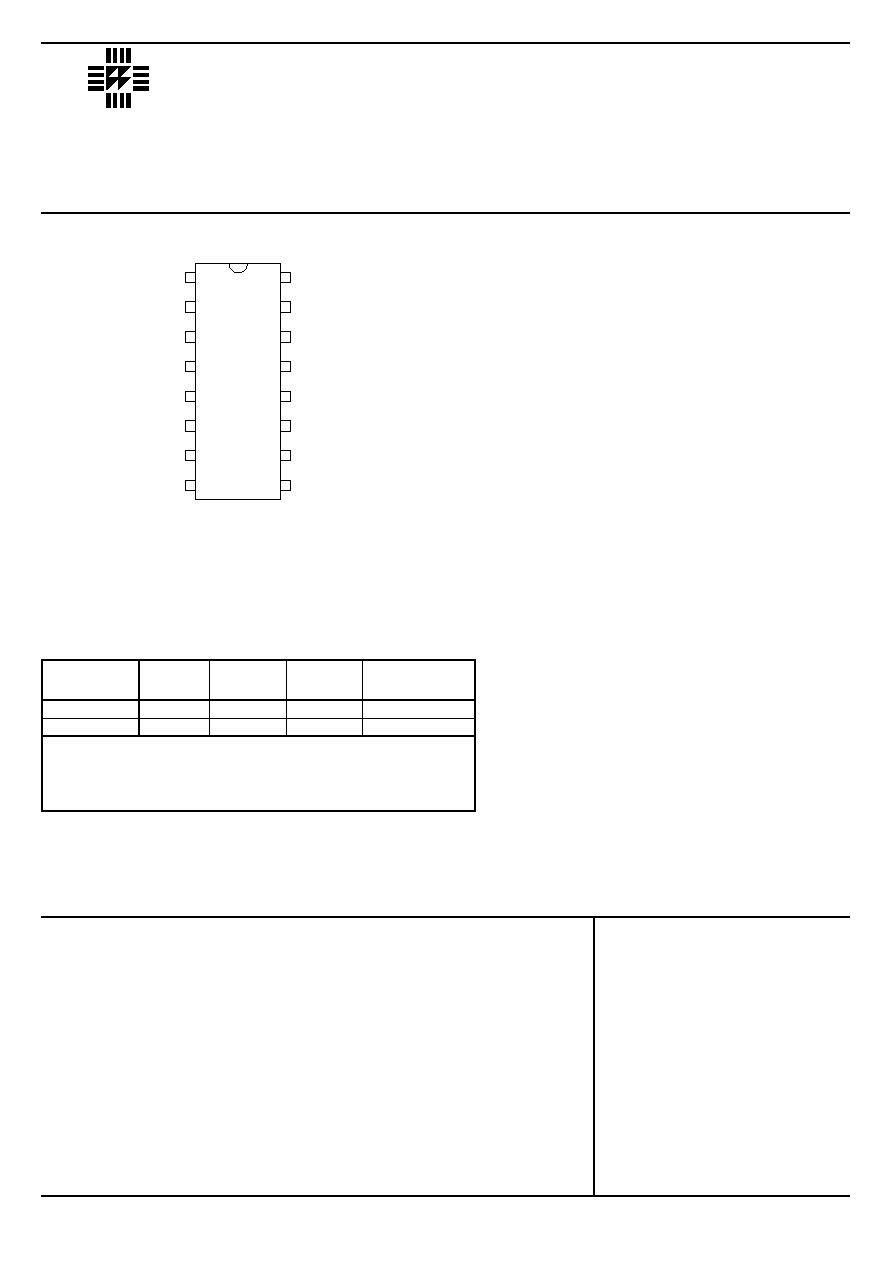
TOP VIEW
J Package ≠ 16 Pin Ceramic DIP
N Package ≠ 16 Pin Plastic DIP
D Package ≠ 16 Pin Plastic (300) SOIC
SCR TRIGGER
REMOTE
ACTIVATE
RESET
O.V. INDICATE
O.V. DELAY
O.V. INPUT
U.V. INPUT
U.V. DELAY
U.V. INDICATE
C.L. INV. INPUT
C.L. NON≠INV. INPUT
OFFSET/COMP
C.L. OUTPUT
GND
V
V
IN
R E F
1
2
3
4
5
6
7
8
16
15
14
13
12
11
10
9
Part J≠Pack
N≠Pack
D≠16
Temp.
Number
16 Pin
16 Pin
16 Pin
Range
IP1543
-55 to +125∞C
IP3543
0 to +70∞C
Order Information
Note:
To order, add the package identifier to the part number.
eg.
IP1543J
IP3543D≠16

LAB
SEME
IP1543 SERIES
Semelab plc.
Telephone (01455) 556565. Telex: 341927. Fax (01455) 552612.
Prelim. 1/96
U.V. INDICATE
9
7
U.V.
V
IN
U.V. DELAY
8
250
µ
A
U.V. SENSE
15
V
REF
O.V. DELAY
5
250
µ
A
O.V.
16
V
IN
2.5 V REF.
14
GND
6
O.V. SENSE
SCR TRIGGER
1
O.V. INDICATE
4
REMOTE
ACTIVATE
2
RESET
3
C.L. OUTPUT
13
C.L.
10
C.L. INV.
V
IN
OFFSET / COMP
12
11
C.L. NON≠INV.
+4.5 to +40V
0 to V
IN
≠ 3
0 to 10mA
0 to 10mA
≠55 to +125∞C
0 to +70∞C
RECOMMENDED OPERATING CONDITIONS
V
IN
Input Supply Voltage
Input Voltage Range
Reference Load Current
Indicate Output Current
Operating Ambient Temperature Range
IP1543
IP3543
DESCRIPTION
The IP1543 and IP3543 power supply supervisory circuits contain all the functions necessary to monitor and control the
output of a sophisticated power supply system. Included on the chip are over-voltage (O.V.) sensing with externally
programmable delay used to trigger an external SCR "Crowbar", under-voltage (U.V.) sensing with externally
programmable delay used to sense either the power supply output or the line input voltage, a third op-amp/comparator
with provision for external compensation and/or offset programming used for either current limiting or as an additional
voltage monitor, and a voltage reference trimmed to ±1%.
BLOCK DIAGRAM
4.5
40
7
10
2.45
2.5
2.55
2.4
2.6
1
5
1
10
12
25
40
50
100
200
400
12
13
0
0.1
≠0.1
≠0.8
1.5
6
≠0.1
≠0.8
1.5
6
400
300
500
2.4
2.5
2.6
2.35
2.65
25
≠0.3
≠1
0.2
0.5
6
8
200
250
300
4.5
40
7
10
2.48
2.5
2.52
2.45
2.55
1
5
1
10
12
25
40
50
100
200
400
12
13
0
0.1
≠0.1
≠0.8
1.5
6
≠0.1
≠0.8
1.5
6
400
300
500
2.45
2.5
2.55
2.4
2.6
25
≠0.3
≠1
0.2
0.5
6
8
200
250
300
Input Voltage Range
Supply Current
Output Voltage
Line Regulation
Load Regulation
Short Circuit Current
Temperature Stability
Peak Output Current
Peak Output Voltage
Output Off Voltage
Remote Activate Current
Remote Activate Voltage
Reset Current
Reset Voltage
Output Current Rise Time
Prop. Delay from Pin 2
Prop. Delay from Pin 6
Input Threshold
(Input Voltage
Rising on Pin 6, Falling on Pin 7)
Input Hysteresis
Input Bias Current
Delay Saturation
Delay High Level
Delay Charging Current
V
IN
= 40V
T
J
= 25∞C
V
IN
= 4.5 to 30V
I
REF
= 0 to 10mA
V
REF
= 0
V
IN
= 5V
R
G
= 0
V
O
= 0
V
IN
= 15V
I
O
= 100mA
V
IN
= 40V
Pin 2 = Gnd
Pin 2 = Open
Pin 3 = Gnd
Pin 2 = Gnd
Pin 3 = Open
Pin 2 = Gnd
R
L
= 50
T
J
= 25∞C
C
D
= 0
V
PIN2
= 0.4V
T
J
= 25∞C
V
PIN6
= 2.7V
T
J
= 25∞C
T
J
= 25∞C
T
J
= 25∞C
Sense Input = 0V
V
D
= 0
LAB
SEME
IP1543 SERIES
Semelab plc.
Telephone (01455) 556565. Telex: 341927. Fax (01455) 552612.
Prelim. 1/96
IP1543
IP3543
Parameter
Test Conditions
Min.
Typ.
Max.
Min.
Typ.
Max.
Units
ELECTRICAL CHARACTERISTICS
(T
J
= Over Operating Temperature Range unless otherwise stated)
V
mA
V
mV
mA
ppm/∞C
mA
V
mA
V
mA
V
mA/
µ
s
ns
ns
V
mV
µ
A
V
µ
A
REFERENCE SECTION
SCR TRIGGER SECTION
COMPARATOR SECTIONS
I
L
= ≠10mA
V
IND
= 40V
V
PIN6
= 2.7V
V
PIN7
= 2.3V
C
D
= 0
T
J
= 25∞C
V
PIN6
= 2.7V
V
PIN7
= 2.3V
C
D
= 0
T
J
= 25∞C
Pin 12 = Open
V
CM
= 0
Pin 12 = Open
V
CM
= 0
10k
from Pin 12 to Gnd
V
CM
= 0 to 12V
V
IN
= 15V
Pin 12 = Open
V
CM
= 0
I
L
= ≠10mA
V
IND
= 40V
A
V
= 0dB
T
J
= 25∞C
V
overdrive
= 100mV
T
J
= 25∞C
Indicate Saturation
Indicate Leakage
Propagation Display
Input Voltage Range
Input Bias Current
Input Offset Voltage
CMRR
AVOL
Output Saturation
Output Leakage
Small Signal Bandwidth
Propagation Delay
IP1543
IP3543
Parameter
Test Conditions
Min.
Typ.
Max.
Min.
Typ.
Max.
Units
0.2
0.5
0.01
1
400
10
0
V
IN
≠ 3
≠0.3
≠1
0
15
70
100
130
60
70
72
80
0.2
0.5
0.01
1
5
200
0.2
0.5
0.01
1
400
10
0
V
IN
≠ 3
≠0.3
≠1
0
10
70
100
130
60
70
72
80
0.2
0.5
0.01
1
5
200
V
µ
A
ns
ms
V
µ
A
mV
dB
V
µ
A
MHz
ns
LAB
SEME
IP1543 SERIES
Semelab plc.
Telephone (01455) 556565. Telex: 341927. Fax (01455) 552612.
Prelim. 1/96
NOTES
1. Test Conditions unless otherwise stated:
V
IN
= 10V
T
J
= ≠55 to +125∞C
for IP1543
T
J
= 0 to +70∞C
for IP3543
ELECTRICAL CHARACTERISTICS
(T
J
= Over Operating Temperature Range unless otherwise stated)
COMPARATOR SECTIONS (cont.)
CURRENT LIMIT SECTION

LAB
SEME
IP1543 SERIES
Semelab plc.
Telephone (01455) 556565. Telex: 341927. Fax (01455) 552612.
Prelim. 1/96
SCR
TRIGGER
GROUND
2.5V
REF.
14
MAIN POSITIVE
SUPPLY
16
15
U.V.
O.V.
7
6
9
4
2
3
1
339 QUAD COMP.
ADDITIONAL
POSITIVE
SUPPLY
NEGATIVE
SUPPLY
VOLTAGE
TO SHUTDOWN
CIRCUIT
R
1
R
2
R
4
R
5
R
6
MASTER POWER SUPPLY
CONDITION INDICATOR
IP1543
BIAS SUPPLY
TO 339 COMPARATORS
R
3
R
7
APPLICATIONS INFORMATION
16
POWER SUPPLY
2.5V
REF.
14
15
R
SC
C.L.
10
11
12
13
TO VOLTAGE
CONTROL LOOP
7
6
5
8
9
4
OUT OF TOLERANCE
INDICATORS
R
1
C
S
R
3
R
6
R
2
R
4
R
5
U.V.
O.V.
C
D1
C
D2
SCR
TRIGGER
2
LATCH
3
RESET
1
R
G
TO SYSTEM
CONTROL
SCR
"CROWBAR"
Typical Application
Sensing Multiple Supply Voltages
Current Limit V
TH
1000
R
1
C
S
is determined by the current loop dynamics.
Peak Current to load I
P
+
V
TH
R
SC
2.5 (R
4
+ R
5
+ R
6
)
R
5
+ R
6
V
O
R
SC
R
2
R
2
+ R
3
Low Output Voltage Limit V
O(low)
=
High Output Voltage Limit V
O(high)
=
Voltage Sensing Delay T
D
= 10000 C
D
SCR trigger power limiting resistor R
G
>
2.5 (R
4
+ R
5
+ R
6
)
R
6
V
IN
-5
0.2