DESCRIPTION
The IP140MA and IP78M00A series of voltage
regulators are fixed output regulators intended for
local, on-card voltage regulation. These devices are
available in 5, 12, and 15 volt options and are
capable of delivering in excess of 500mA over
temperature.
The A-suffix devices are fully specified at 0.5A,
provide 0.01% / V line regulation, 0.3% / A load
regulation, and ±1% output voltage tolerance at room
temperature. Protection features include safe
operating area, current limiting and thermal
shutdown.
Order Information
Part H≠Pack
J≠Pack
SG≠Pack
Temp.
Number
(TO≠39)
CERDIP
SMD
Range
IP78MxxAzz
-55 to +150∞C
IP78Mxxzz
"
IP140MAzz≠xx
"
IP140Mzz≠xx
"
Note:
xx = Voltage Code
(05, 12, 15)
eg.
IP78M05J
zz = Package Code
(H, J, SG)
IP140MAH≠12
IP140MA SERIES
IP140M
SERIES
IP78M00A SERIES
IP78M00
SERIES
Prelim.7/00
Semelab plc.
Telephone +44(0)1455 556565. Fax +44(0)1455 552612.
E-mail:
sales@semelab.co.uk
Website:
http://www.semelab.co.uk
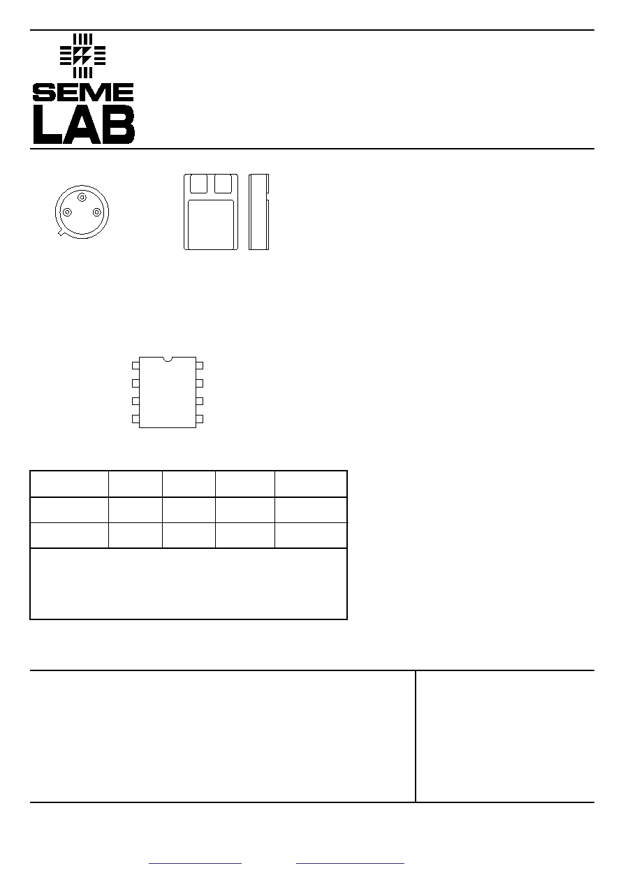
Pin 1 ≠ V
IN
Pin 2 ≠ V
OUT
Case ≠ Ground
H Package ≠ TO≠39
1
2
3
8 Pin J Package
4
5
1
2
3
8
7
6
NC
NC
NC
OUT
V
IN
V
NC
GND
NC
0.5 AMP
POSITIVE
VOLTAGE REGULATOR
FEATURES
∑ OUTPUT CURRENT UP TO 0.5A
∑ OUTPUT VOLTAGES OF 5, 12, 15V
∑ 0.01% / V LINE REGULATION
∑ 0.3% / A LOAD REGULATION
∑ THERMAL OVERLOAD PROTECTION
∑ SHORT CIRCUIT PROTECTION
∑ OUTPUT TRANSISTOR SOA PROTECTION
∑ 1% VOLTAGE TOLERANCE (≠A VERSIONS)
V
I
DC Input Voltage
(for V
O
= 5, 12, 15V)
P
D
Power Dissipation
R
q
JC
Thermal Resistance Junction to Case
≠ H Package
R
q
JC
Thermal Resistance Junction to Case
≠ SG Package
R
q
JA
Thermal Resistance Junction to Ambient
≠ J Package
T
J
Operating Junction Temperature Range
T
stg
Storage Temperature
35V
Internally limited
1
20∞C / W
TBA ∞C / W
119∞C / W
≠55 to 150∞C
≠65 to 150∞C
ABSOLUTE MAXIMUM RATINGS
(T
C
= 25∞C unless otherwise stated)
Note 1. Although power dissipation is internally limited, these specifications are applicable for maximum power dissipation
P
MAX
of 2W for the H≠Package ,1.05W for the J≠Package and 15W for the SG≠Package.
Pin 1 ≠ V
IN
Pin 2 ≠ Ground
Pin 3 ≠ V
OUT
SMD 1
CERAMIC SURFACE MOUNT
!
V
O
Output Voltage
D
V
O
Line Regulation
D
V
O
Load Regulation
I
Q
Quiescent Current
D
I
Q
Quiescent Current
Change
V
N
Output Noise
Voltage
D
V
IN
Ripple Rejection
D
V
O
Dropout Voltage
I
sc
Short Circuit Current
I
pk
Peak Output Current
Average Temperature
Coefficient of V
O
IP78M05A
IP78M05
IP140MA≠05
IP140M≠05
Parameter
Test Conditions
Min.
Typ.
Max.
Min.
Typ.
Max.
Units
I
O
= 100mA
V
IN
= 10V
I
O
= 5mA to 350mA
P
D
£
P
MAX
V
IN
= 7.5V to 20V
T
J
= -55 to 150∞C
V
IN
= 7V to 25V
I
O
= 200mA
V
IN
= 8V to 25V
T
J
= -55 to 150∞C
I
O
= 500mA
V
IN
= 8V to 12V
I
O
= 5mA to 500mA
V
IN
= 10V
T
J
= -55 to 150∞C
V
IN
= 10V
I
O
= 350mA
T
J
= -55 to 150∞C
I
O
= 5mA to 500mA
V
IN
= 10V
T
J
= -55 to 150∞C
I
O
= 200mA
V
IN
= 8V to 25V
T
J
= -55 to 150∞C
f = 10Hz to 100kHz
I
O
= 300mA
f = 120Hz
I
O
= 100mA
V
IN
= 8V to 18V
T
J
= -55 to 150∞C
I
O
= 350mA
V
IN
= 35V
V
IN
= 10V
I
O
= 5mA
IP140MA SERIES
IP140M
SERIES
IP78M00A SERIES
IP78M00
SERIES
Prelim.7/00
Semelab plc.
Telephone +44(0)1455 556565. Fax +44(0)1455 552612.
E-mail:
sales@semelab.co.uk
Website:
http://www.semelab.co.uk
4.8
5
5.2
4.75
5.25
50
25
50
50
4
6
0.5
0.8
40
200
62
62
2.5
300
600
0.7
1.0
1.6
0.5
4.95
5
5.05
4.85
5.15
3
10
3
10
3
10
5
50
4
6
0.1
0.5
0.2
0.8
40
200
65
80
65
80
2
2.5
300
600
0.7
1.0
1.4
0.5
2.0
V
mV
mV
mA
mA
m
V
dB
V
mA
A
mV
∞C
1) All characteristics are measured with a capacitor across the input of 0.22
m
F and a capacitor across the output of 0.1
m
F.
All characteristics except noise voltage and ripple rejection ratio are measured using pulse techniques (t
p
£
10ms,
d £
5%). Output
voltage changes due to changes in internal temperature must be taken into account separately.
2) Test Conditions unless otherwise stated: T
J
= 25∞C
P
MAX
= 2W for H Package (TO≠39)
P
MAX
= 1.05W for J Package (CERDIP)
P
MAX
= 15W for SG Package (SMD1)
ELECTRICAL CHARACTERISTICS

V
O
Output Voltage
D
V
O
Line Regulation
D
V
O
Load Regulation
I
Q
Quiescent Current
D
I
Q
Quiescent Current
Change
V
N
Output Noise
Voltage
D
V
IN
Ripple Rejection
D
V
O
Dropout Voltage
I
sc
Short Circuit Current
I
pk
Peak Output Current
Average Temperature
Coefficient of V
O
IP78M12A
IP78M12
IP140MA≠12
IP140M≠12
Parameter
Test Conditions
Min.
Typ.
Max.
Min.
Typ.
Max.
Units
I
O
= 100mA
V
IN
= 19V
I
O
= 5mA to 350mA
P
D
£
P
MAX
V
IN
= 14.8V to 27V
T
J
= -55 to 150∞C
I
O
= 200mA
V
IN
= 14.5V to 30V
V
IN
= 16V to 30V
T
J
= -55 to 150∞C
I
O
= 500mA
V
IN
= 16V to 22V
I
O
= 5mA to 500mA
V
IN
= 19V
T
J
= -55 to 150∞C
V
IN
= 19V
I
O
= 350mA
T
J
= -55 to 150∞C
I
O
= 5mA to 500mA
V
IN
= 19V
T
J
= -55 to 150∞C
I
O
= 200mA
V
IN
= 14.8V to 30V
T
J
= -55 to 150∞C
f = 10Hz to 100kHz
I
O
= 300mA
f = 120Hz
I
O
= 100mA
V
IN
= 15V to 25V
T
J
= -55 to 150∞C
I
O
= 350mA
V
IN
= 35V
V
IN
= 19V
I
O
= 5mA
11.50
12
12.50
11.40
12.60
60
30
120
120
4
6
0.5
0.8
75
480
55
55
2.5
300
600
0.7
1.0
1.6
1.2
11.88
12
12.12
11.64
12.36
4
18
4
18
4
18
10
60
4
6
0.1
0.5
0.2
0.8
75
480
58
72
58
72
2
2.5
300
600
0.7
1.0
1.4
1.2
4.8
V
mV
mV
mA
mA
m
V
dB
V
mA
A
mV
∞C
1) All characteristics are measured with a capacitor across the input of 0.22
m
F and a capacitor across the output of 0.1
m
F.
All characteristics except noise voltage and ripple rejection ratio are measured using pulse techniques (t
p
£
10ms,
d £
5%). Output
voltage changes due to changes in internal temperature must be taken into account separately.
2) Test Conditions unless otherwise stated: T
J
= 25∞C
P
MAX
= 2W for H Package (TO≠39)
P
MAX
= 1.05W for J Package (CERDIP)
P
MAX
= 15W for SG Package (SMD1)
ELECTRICAL CHARACTERISTICS
IP140MA SERIES
IP140M
SERIES
IP78M00A SERIES
IP78M00
SERIES
Prelim.7/00
Semelab plc.
Telephone +44(0)1455 556565. Fax +44(0)1455 552612.
E-mail:
sales@semelab.co.uk
Website:
http://www.semelab.co.uk

V
O
Output Voltage
D
V
O
Line Regulation
D
V
O
Load Regulation
I
Q
Quiescent Current
D
I
Q
Quiescent Current
Change
V
N
Output Noise
Voltage
D
V
IN
Ripple Rejection
D
V
O
Dropout Voltage
I
sc
Short Circuit Current
I
pk
Peak Output Current
Average Temperature
Coefficient of V
O
IP78M15A
IP78M15
IP140MA≠15
IP140M≠15
Parameter
Test Conditions
Min.
Typ.
Max.
Min.
Typ.
Max.
Units
I
O
= 100mA
V
IN
= 23V
I
O
= 5mA to 350mA
P
D
£
P
MAX
V
IN
= 18V to 30V
T
J
= -55 to 150∞C
V
IN
= 17.5V to 30V
I
O
= 200mA
V
IN
= 20V to 30V
T
J
= -55 to 150∞C
I
O
= 500mA
V
IN
= 20V to 26V
I
O
= 5mA to 500mA
V
IN
= 23V
T
J
= -55 to 150∞C
V
IN
= 23V
I
O
= 350mA
T
J
= -55 to 150∞C
I
O
= 5mA to 500mA
V
IN
= 23V
T
J
= -55 to 150∞C
I
O
= 200mA
V
IN
= 18V to 30V
T
J
= -55 to 150∞C
f = 10Hz to 100kHz
f = 120Hz
I
O
= 300mA
V
IN
= 18.5V to
I
O
= 100mA
28.5V
T
J
= -55 to 150∞C
I
O
= 350mA
V
IN
= 35V
V
IN
= 23V
I
O
= 5mA
14.40
15
15.60
14.25
15.75
60
30
150
150
4
6
0.5
0.8
90
600
54
54
2.5
300
600
0.7
1.0
1.6
1.5
14.85
15
15.15
14.55
15.45
4
22
4
22
4
22
12
75
4
6
0.1
0.5
0.2
0.8
90
600
57
70
57
70
2
2.5
300
600
0.7
1.0
1.4
1.5
6.0
V
mV
mV
mA
mA
m
V
dB
V
mA
A
mV
∞C
1) All characteristics are measured with a capacitor across the input of 0.22
m
F and a capacitor across the output of 0.1
m
F.
All characteristics except noise voltage and ripple rejection ratio are measured using pulse techniques (t
p
£
10ms,
d £
5%). Output
voltage changes due to changes in internal temperature must be taken into account separately.
2) Test Conditions unless otherwise stated: T
J
= 25∞C
P
MAX
= 2W for H Package (TO≠39)
P
MAX
= 1.05W for J Package (CERDIP)
P
MAX
= 15W for SG Package (SMD1)
ELECTRICAL CHARACTERISTICS
IP140MA SERIES
IP140M
SERIES
IP78M00A SERIES
IP78M00
SERIES
Prelim.7/00
Semelab plc.
Telephone +44(0)1455 556565. Fax +44(0)1455 552612.
E-mail:
sales@semelab.co.uk
Website:
http://www.semelab.co.uk