
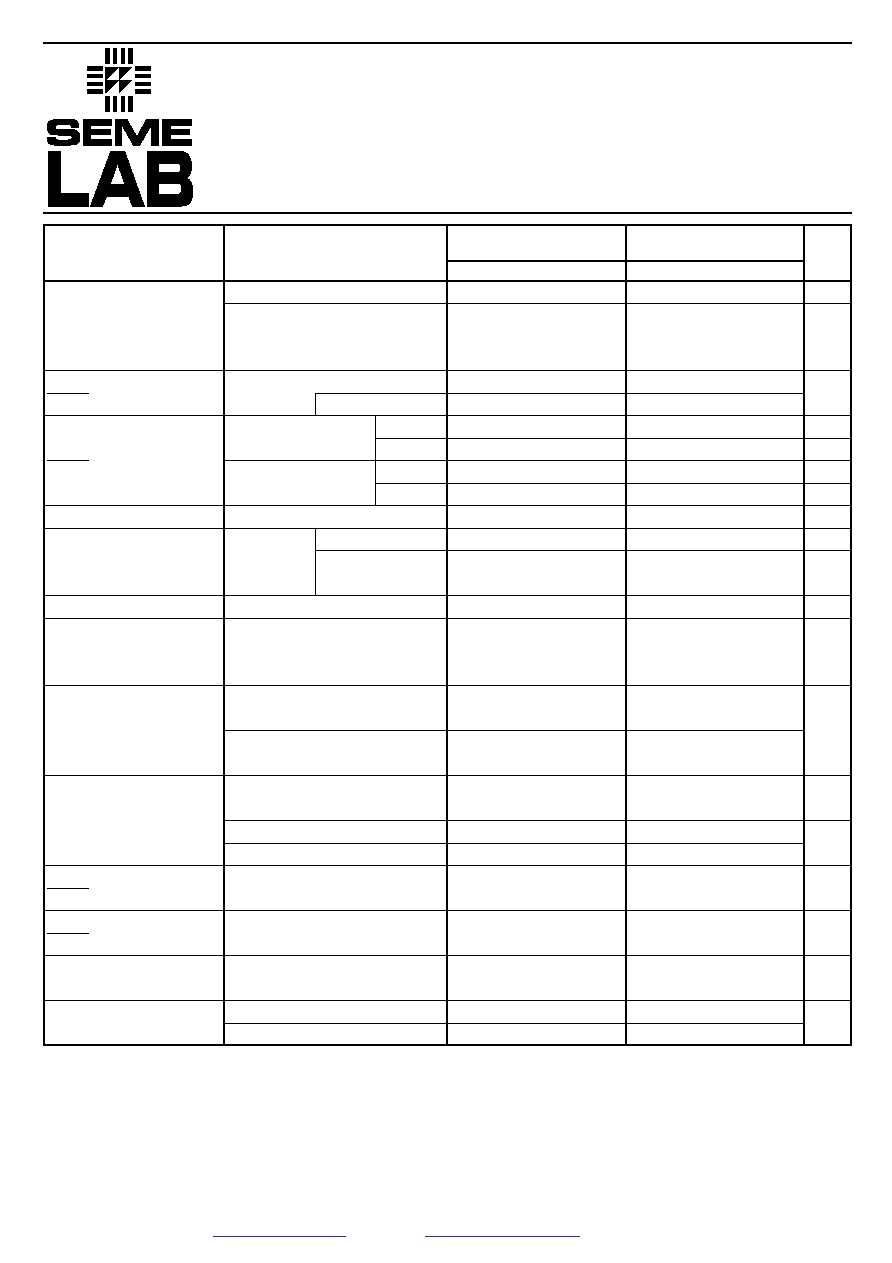
Pin 1 ≠ ADJ.
Pin 2 ≠ V
OUT
Pin 3 ≠ V
IN
SMD1
CERAMIC SURFACE
MOUNT
Pin 1 ≠ ADJ.
Pin 2 ≠ V
OUT
Pin 3 ≠ V
IN
Case ≠ V
OUT
G Package ≠ TO257
Pin 1 ≠ ADJ.
Pin 2 ≠ V
IN
Case ≠ V
OUT
K Package ≠ TO3
Pin 1 ≠ ADJ.
Pin 2 ≠ V
IN
Case ≠ V
OUT
R Package ≠ TO66
Prelim. 8/00
Semelab plc.
Telephone +44(0)1455 556565. Fax +44(0)1455 552612.
E-mail:
sales@semelab.co.uk
Website:
http://www.semelab.co.uk
IP117, IP117A
IP317, IP317A
LM117, LM117A
1.5 AMP
POSITIVE ADJUSTABLE
VOLTAGE REGULATOR
FOR HI-REL APPLICATIONS
40V
60V
Internally limited
Internally limited
See Table Above
≠65 to 150∞C
ABSOLUTE MAXIMUM RATINGS
(T
case
= 25∞C unless otherwise stated)
FEATURES
∑ Output voltage range of:
1.25 to 40V for standard version
1.25 to 60V for HV version
∑ Output voltage tolerance 1%
∑ Load regulation 0.3%
∑ Line regulation 0.01%/V
∑ Complete series of protections:
current limiting
thermal shutdown
soa control
∑ Also available in TO220 metal
isolated package (1mm pins)
1
2
3
3
1
2
Pin 1 ≠ ADJ.
Pin 2 ≠ V
OUT
Pin 3 ≠ V
IN
T Package ≠ TO220 Plastic
1
2
3
1 2 3
Pin 1 ≠ ADJ.
Pin 2 ≠ V
OUT
Pin 3 ≠ V
IN
Case
≠
Isolated
IG Package ≠ TO257
Pin 1 ≠ ADJ.
Pin 2 ≠ V
OUT
Pin 3 ≠ V
IN
SMD05
CERAMIC SURFACE
MOUNT
1 2 3
!
V
I≠O
Input - Output Differential Voltage
≠ Standard
≠ HV Series
I
O
Output Current
P
D
Power Dissipation
T
J
Operating Junction Temperature Range
T
STG
Storage Temperature
!
Prelim. 8/00
Semelab plc.
Telephone +44(0)1455 556565. Fax +44(0)1455 552612.
E-mail:
sales@semelab.co.uk
Website:
http://www.semelab.co.uk
IP117, IP117A
IP317, IP317A
LM117, LM117A
1) Regulation is measured at constant junction temperature, using pulse testing at a low duty cycle. Changes in output voltage due to heating effects
are covered under thermal regulation specifications. Load regulation is measured from the bottom of the package for the TO≠3 and TO≠66 pack-
ages, at the junction of the wide and narrow portion of the output lead for the TO≠220 package, and
1
/
8
" below the base of the package on the out-
put pin of the TO≠257 package.
2) Test Conditions unless othewise stated:
V
IN
≠ V
OUT
= 5V , T
J
= 25∞C , I
OUT
= 0.5A , I
MAX
= 1.5A.
P
MAX
= 10W for SMD1, 20W for all other package styles.
V
MAX
= 40V for standard series , 60V for HV series.
1.238
1.25
1.262
1.225
1.250
1.270
0.005
0.010
0.010
0.020
5
15
0.1
0.3
15
50
0.3
1
0.002
0.020
65
66
80
50
100
0.2
5
3.5
5
3.5
7
1.5
2.2
0.30
0.50
0.10
1
2
0.3
1
0.001
2.3
3
5
7
3
5
1.200
1.250
1.300
0.010
0.020
0.020
0.050
5
15
0.1
0.3
20
50
0.3
1
0.030
0.070
65
66
80
50
100
0.2
5
3.5
5
3.5
7
1.5
2.2
0.30
0.50
0.10
1
0.3
1
0.001
2.3
3
5
7
3
5
IP117A , IP117AHV
IP117 , IP117HV
LM117A , LM117AHV
LM117 , LM117HV
Parameter
Test Conditions
Min.
Typ.
Max.
Min.
Typ.
Max. Units
V
REF
Reference Voltage
D
V
OUT
Line Regulation
1
D
V
IN
D
V
OUT
Load Regulation
1
D
I
OUT
Thermal Regulation
Ripple Rejection
I
ADJ
Adjust Pin Current
D
I
ADJ
Adjust Pin Current
Change
I
MIN
Minimum Load
Current
I
CL
Current Limit
D
V
OUT
Temperature
D
TEMP Stability
D
V
OUT
Long Term Stability
D
TIME
e
n
RMS Output Noise
(% of V
OUT
)
R
q
JC
Thermal Resistance
Junction to Case
I
OUT
= 10mA
I
OUT
= 10mA to I
MAX
V
IN
≠ V
OUT
= 3V to V
MAX
P
£
P
MAX
T
J
= ≠55 to +150∞C
V
IN
≠ V
OUT
= 3V to V
MAX
T
J
= ≠55 to +150∞C
I
OUT
= 10mA to I
MAX
V
OUT
£
5V
V
OUT
≥
5V
I
OUT
= 10mA to I
MAX
V
OUT
£
5V
T
J
= ≠55 to +150∞C
V
OUT
≥
5V
t
p
= 20ms
C
ADJ
= 0
V
OUT
= 10V
C
ADJ
= 10
m
F
f = 120Hz
T
J
= ≠55 to +150∞C
T
J
= ≠55 to +150∞C
I
OUT
= 10mA to I
MAX
T
J
= ≠55 to +150∞C
V
IN
≠ V
OUT
= 2.5V to V
MAX
V
IN
≠ V
OUT
= 40V
T
J
= ≠55 to +150∞C
V
IN
≠ V
OUT
= 60V
(HV SERIES)
T
J
= ≠55 to +150∞C
V
IN
≠ V
OUT
£
15V
T
J
= ≠55 to +150∞C
V
IN
≠ V
OUT
= 40V
V
IN
≠ V
OUT
= 60V
(HV SERIES)
T
J
= ≠55 to +150∞C
T
A
= +125∞C
t = 1000 Hrs
f = 10 Hz to 10 kHz
K Package
R Package
G, IG Packages
V
V
% / V
mV
%
mV
%
%/W
dB
dB
m
A
m
A
mA
A
A
%
%
%
∞C/W
Prelim. 8/00
Semelab plc.
Telephone +44(0)1455 556565. Fax +44(0)1455 552612.
E-mail:
sales@semelab.co.uk
Website:
http://www.semelab.co.uk
IP117, IP117A
IP317, IP317A
LM117, LM117A
1) Regulation is measured at constant junction temperature, using pulse testing at a low duty cycle. Changes in output voltage due to heating effects
are covered under thermal regulation specifications. Load regulation is measured from the bottom of the package for the TO≠3 and TO≠66 pack-
ages, at the junction of the wide and narrow portion of the output lead for the TO≠220 package, and
1
/
8
" below the base of the package on the out-
put pin of the TO≠257 package.
2) Test Conditions unless othewise stated:
V
IN
≠ V
OUT
= 5V , T
J
= 25∞C , I
OUT
= 0.5A , P
MAX
= 20W , I
MAX
= 1.5A
V
MAX
= 40V for standard series , 60V for HV series.
1.238
1.25
1.262
1.225
1.25
1.270
0.005
0.010
0.010
0.020
5
25
0.1
0.5
15
50
0.3
1
0.002
0.020
65
66
80
50
100
0.2
5
3.5
10
3.5
12
1.5
2.2
0.15
0.40
0.10
1
2
0.3
1
0.003
2.3
3
4
5
1.200
1.250
1.300
0.010
0.040
0.020
0.070
5
25
0.1
0.5
20
70
0.3
1.5
0.030
0.070
65
66
80
50
100
0.2
5
3.5
10
3.5
12
1.5
2.2
0.15
0.40
0.10
1
0.3
1
0.003
2.3
3
5
7
IP317A
IP317
IP317AHV
IP317HV
Parameter
Test Conditions
Min.
Typ.
Max.
Min.
Typ.
Max. Units
V
REF
Reference Voltage
D
V
OUT
Line Regulation
1
D
V
IN
D
V
OUT
Load Regulation
1
D
I
OUT
Thermal Regulation
Ripple Rejection
I
ADJ
Adjust Pin Current
D
I
ADJ
Adjust Pin Current
Change
I
MIN
Minimum Load
Current
I
CL
Current Limit
D
V
OUT
Temperature
D
TEMP Stability
D
V
OUT
Long Term Stability
D
TIME
e
n
RMS Output Noise
(% of V
OUT
)
R
q
JC
Thermal Resistance
Junction to Case
I
OUT
= 10mA
I
OUT
= 10mA to I
MAX
V
IN
≠ V
OUT
= 3V to V
MAX
P
£
P
MAX
T
J
= 0 to 125∞C
V
IN
≠ V
OUT
= 3V to V
MAX
T
J
= 0 to 125∞C
I
OUT
= 10mA to I
MAX
V
OUT
£
5V
V
OUT
≥
5V
I
OUT
= 10mA to I
MAX
V
OUT
£
5V
T
J
= ≠55 to +150∞C
V
OUT
≥
5V
t
p
= 20ms
C
ADJ
= 0
V
OUT
= 10V
C
ADJ
= 10
m
F
f = 120Hz
T
J
= 0 to 125∞C
T
J
= 0 to 125∞C
I
OUT
= 10mA to I
MAX
T
J
= 0 to 125∞C
V
IN
≠ V
OUT
= 2.5V to V
MAX
V
IN
≠ V
OUT
= 40V
T
J
= 0 to 125∞C
V
IN
≠ V
OUT
= 60V
(HV SERIES)
T
J
= 0 to 125∞C
V
IN
≠ V
OUT
£
15V
T
J
= 0 to 125∞C
V
IN
≠ V
OUT
= 40V
V
IN
≠ V
OUT
= 60V
(HV SERIES)
T
J
= 0 to 125∞C
t = 1000 Hrs
f = 10 Hz to 10 kHz
K Package
T Package
V
V
% / V
mV
%
mV
%
%/W
dB
dB
m
A
m
A
mA
A
A
%
%
%
∞C/W

Improving Ripple Rejection
2816 EEPROM Supply Programmer for
Read/Write Control
Temperature Compensated
Lead≠Acid Battery Charger
Note:
To order, add the package
identifier to the part number.
eg.
IP117AHVK
IP1175SMD05
IP317T
Prelim. 8/00
Semelab plc.
Telephone +44(0)1455 556565. Fax +44(0)1455 552612.
E-mail:
sales@semelab.co.uk
Website:
http://www.semelab.co.uk
IP117, IP117A
IP317, IP317A
LM117, LM117A
249
1%
ADJ
IP317A
V
IN
V
O U T
1
µ
F
+24V
To
750
1%
3.24k
1%
V
PP
39k
18k
100k
To OE
READ
WRITE
BYTE ERASE
CHIP ERASE
All gates 7406.
R1
121
ADJ
IP317A
V
IN
V
O U T
1
µ
F
V
IN
C1
10
µ
F
5V
R2
383
20k
10k
50
2N3906
243
ADJ
IP317A
V
IN
V
O U T
V
IN
1N4001
50k
12V
THERMALLY
COUPLE
Remote Sensing
5V Regulator with Shut Down
OE
V
PP
READ
0V
5V
WRITE
BYTE
5V
21V
CHIP ERASE 12V
21V
APPLICATIONS INFORMATION
C1 improves ripple rejection.
X
C
should be small compared to R2.
IG≠Pack
Part G≠Pack
K≠Pack
R≠Pack
T≠Pack
Temp.
Number
(TO257)
SMD1
SMD05
(TO3)
(TO66)
(TO220)
Range
LM117
-55 to +150∞C
LM117HV
"
LM117A
"
LM117AHV
"
IP117
-55 to +150∞C
IP117HV
"
IP117A
"
IP117AHV
"
LM317
0 to 125∞C
LM317HV
"
IP317
"
IP317HV
"
IP317A
"
IP317AHV
"
Order Information
1k
1k
383
121
ADJ
IP 317A
V
IN
V
O U T
2N3904
TTL
1
µ
F
V
IN
V
O U T
5V
ADJ
IP317A
RETURN
121
383
LM301A
8
6
4
3
2
7
1
25
5
µ
F
1k
25
V
IN
(Max Drop 300mV)
OUTPUT
V
IN
V
IN
V
O U T
R
P
R
L
RETURN