SB08-100M
A
SB08-100AM
SB08-100RM
Document Number 3277
Issue 2
Semelab plc.
Telephone +44(0)1455 556565. Fax +44(0)1455 552612.
E-mail:
sales@semelab.co.uk
Website:
http://www.semelab.co.uk
Semelab Plc reserves the right to change test conditions, parameter limits and package dimensions without notice. Information furnished by Semelab is believed
to be both accurate and reliable at the time of going to press. However Semelab assumes no responsibility for any errors or omissions discovered in its use.
Semelab encourages customers to verify that datasheets are current before placing orders.
V
RRM
Peak Repetitive Reverse Voltage
V
RSM
Peak Non-Repetitive Reverse Voltage
V
R
Continuous Reverse Voltage
I
O
Output Current
I
FSM
Peak Non-Repetitive Surge Current (50Hz)
T
STG
Storage Temperature Range
T
J
Maximum Operating Junction Temperature
100V
100V
100V
8A
275A
-55∞C to 175∞C
175∞C
DUAL SCHOTTKY
BARRIER DIODE IN
TO220 METAL PACKAGE
FOR HI≠REL APPLICATIONS
ABSOLUTE MAXIMUM RATINGS
(T
case
= 25∞C unless otherwise stated)
SB08 - 100M
A
SB08 - 100AM
SB08 - 100RM
FEATURES
∑
HERMETIC TO220 METAL PACKAGE
∑
SCREENING OPTIONS AVAILABLE
∑
OUTPUT CURRENT 16A(8A per leg)
∑
LOW VF
∑
LOW LEAKAGE
∑
ISOLATED CASE
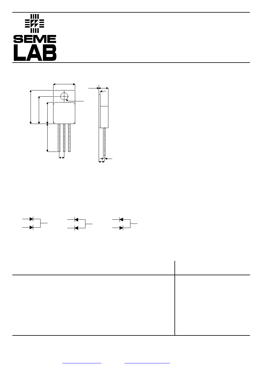
MECHANICAL DATA
Dimensions in mm
16.5 (0.65)
1.5(0.53)
10.6 (0.42)
12.70 (0.50 m
i
n
)
2.54 (0.1)
BSC
3.70 Dia. Nom
1 2 3
0.8
(0.03)
2.70
(0.106)
1.0
(0.039)
4.6 (0.18)
10.6 (0.42)
TO220 (TO-257AB) METAL PACKAGE
SB08-100M
SB08-100AM
SB08-100RM
1
3
2
1
3
2
1
3
2
1 = A1 Anode 1
2 = K Cathode
3 = A2 Anode 2
1 = K1 Cathode 1
2 = A Anode
3 = K2 Cathode 2
1 = K1 Cathode 1
2 = Centre Tap
3 = A2 Anode
Common Cathode
Common Anode
Series Connection
ELECTRICAL CONNECTIONS
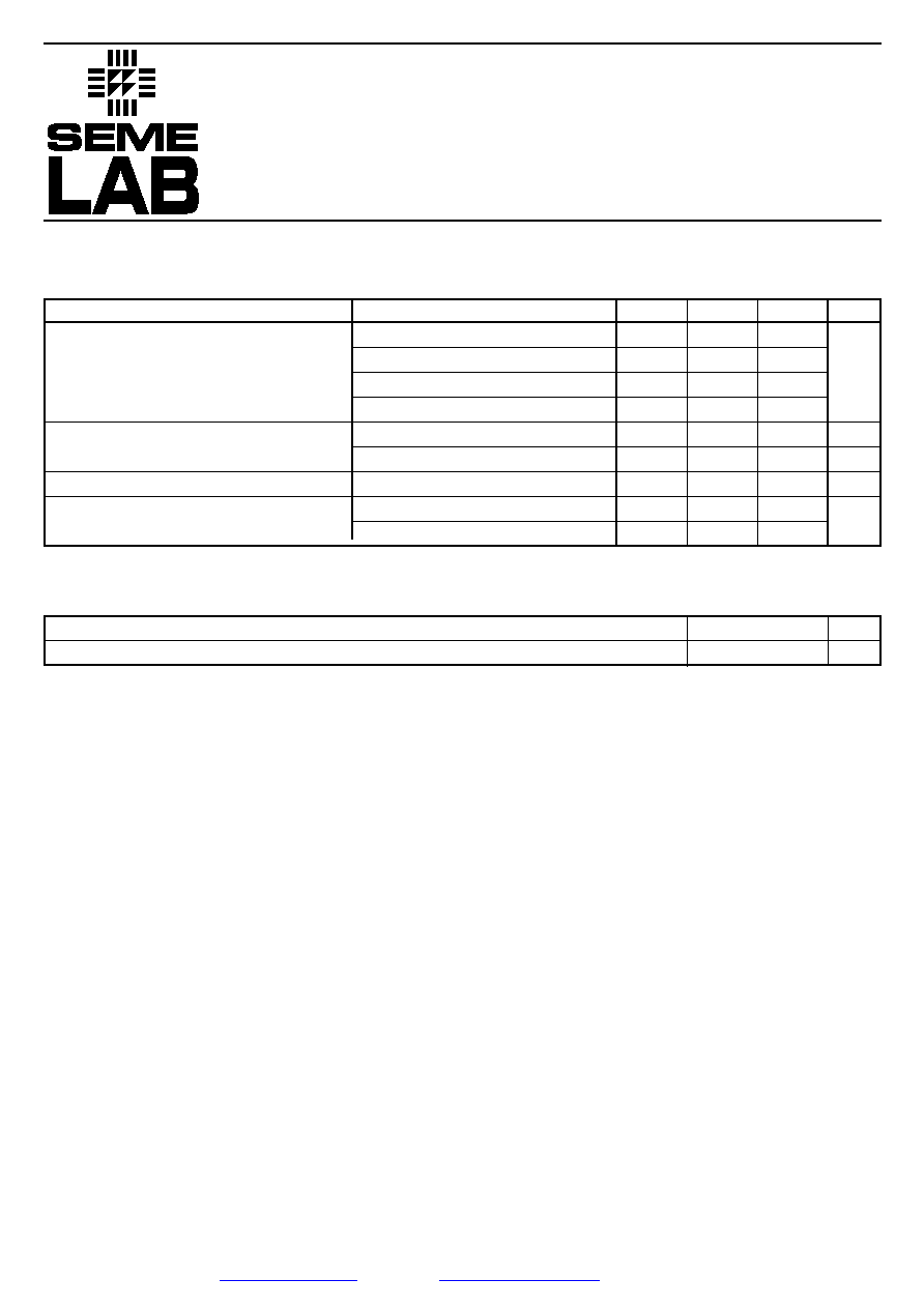
Parameter
Unit
1.5
SB08-100M
A
SB08-100AM
SB08-100RM
Document Number 3277
Issue 2
Semelab plc.
Telephone +44(0)1455 556565. Fax +44(0)1455 552612.
E-mail:
sales@semelab.co.uk
Website:
http://www.semelab.co.uk
Semelab Plc reserves the right to change test conditions, parameter limits and package dimensions without notice. Information furnished by Semelab is believed
to be both accurate and reliable at the time of going to press. However Semelab assumes no responsibility for any errors or omissions discovered in its use.
Semelab encourages customers to verify that datasheets are current before placing orders.
Parameter
Test Conditions
Min.
Typ.
Max.
Unit
V
FM
Max Forward Voltage (per diode)
I
RM
Reverse Current (per diode)
C
T
Junction Capacitance (per diode)
I
F(AV)
Max Average Forward Current
I
F
= 8A*
T
J
= 25∞C
I
F
= 16A*
T
J
= 25∞C
I
F
= 8A*
T
J
= 125∞C
I
F
= 16A*
T
J
= 125∞C
V
R
= V
RRM*
T
J
= 125∞C
V
R
= V
RRM
T
J
= 25∞C
V
R
= 5 V
f = 1 MHz
50% Duty Cycle
Per Diode
50% Duty Cycle
Per Device
0.75
0.95
0.60
0.75
7
550
500
8
16
V
mA
µ
A
pF
A
ELECTRICAL CHARACTERISTICS
(Per Diode) T
CASE
= 25∞C unless otherwise stated
R
TH(j-c)
Maximum Thermal Resistance Junction To Case
∞C/W
*Pulse test tp=300µs
2%