Semelab plc.
Telephone +44(0)1455 556565. Fax +44(0)1455 552612.
E-mail:
sales@semelab.co.uk
Website:
http://www.semelab.co.uk
SML
Parameter
901R1AN
1001R1AN
901R3AN
1001R3AN
Unit
Characteristic / Test Conditions / Part Number
Min.
Typ.
Max. Unit
LAB
SEME
Prelim. 12/00
BV
DSS
I
DSS
I
GSS
I
D(ON)
V
GS(TH)
R
DS(ON)
V
DSS
I
D
I
DM
V
GS
P
D
T
J
, T
STJ
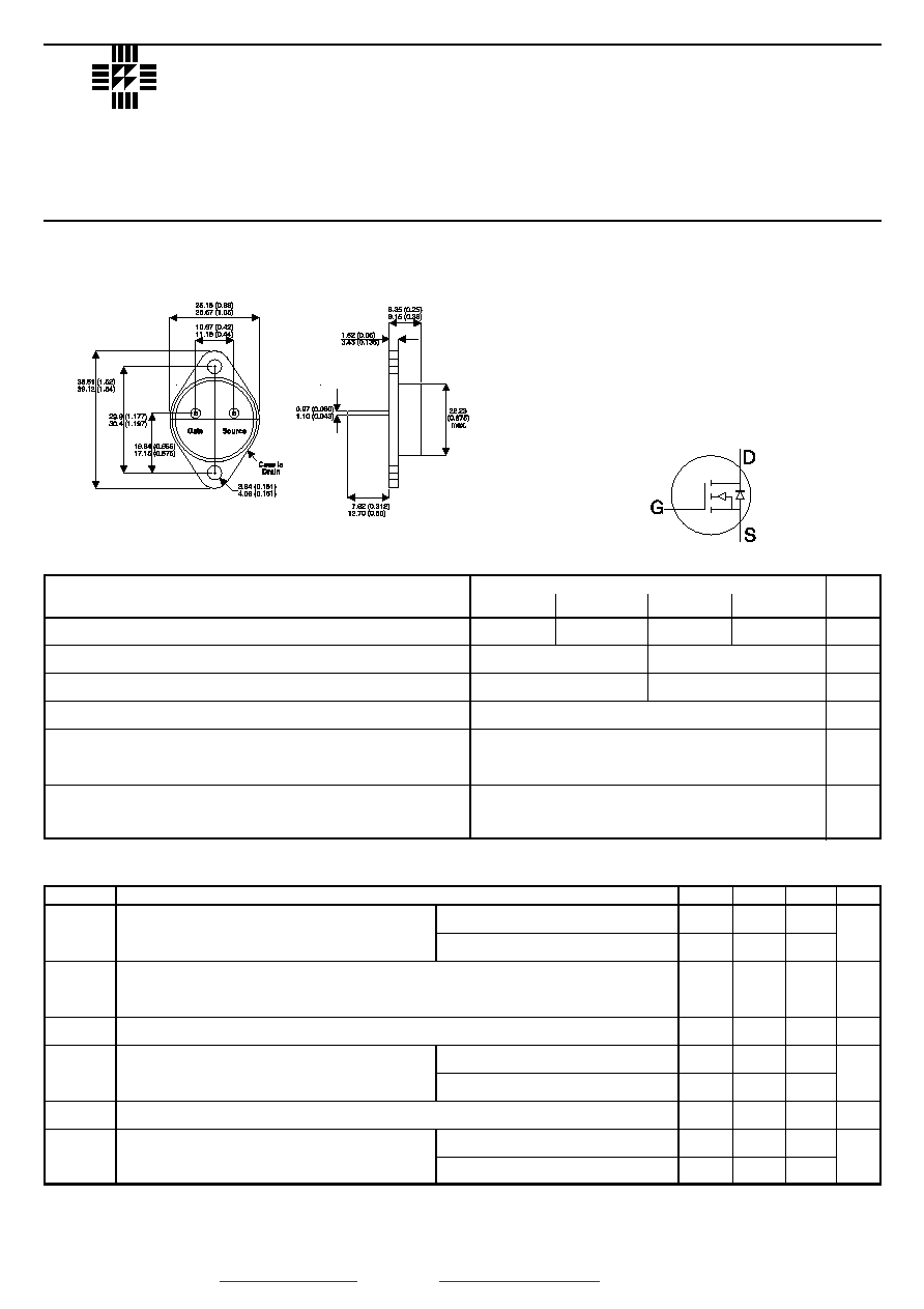
TO3 Package Outline.
Dimensions in mm (Inches)
Drain � Source Voltage
Continuous Drain Current
Pulsed Drain Current
1
Gate � Source Voltage
Total Power Dissipation @ T
case
= 25�C
Derate above 25�C
Operating and Storage Junction Temperature
Range
SML1001R1AN / SML1001R3AN
SML901R1AN / SML901R3AN
(V
GS
= �30V , V
DS
= 0V)
SML1001R1AN / SML901R1AN
SML1001R1AN / SML901R3AN
SML1001R1AN / SML901R1AN
SML1001R3AN / SML901R3AN
POWER MOS IVTM
N�CHANNEL
ENHANCEMENT MODE
HIGH VOLTAGE
POWER MOSFETS
900
1000
900
1000
9.5
8.5
38
34
�30
230
�55 to 150
V
A
A
V
W
�C
Drain � Source Breakdown Voltage
(V
GS
= 0V , I
D
= 250
mA)
Zero Gate Voltage Drain Current
Gate � Source Leakage Current
On State Drain Current
2
(V
DS
> I
D(ON)
x R
DS(ON)
Max , V
GS
= 10V)
Gate Threshold Voltage
Static Drain � Source On State Resistance
2
(V
GS
=10V , I
D
= 0.5 I
D
[Cont.])
1000
900
250
1000
�100
9.5
8.5
2
4
1.1
1.3
V
mA
nA
A
V
W
MAXIMUM RATINGS
(T
case
=25�C unless otherwise stated)
1) Repetitive Rating: Pulse Width limited by maximum junction temperature.
2) Pulse Test: Pulse Width < 380
mS , Duty Cycle < 2%
STATIC ELECTRICAL RATINGS
(T
case
=25�C unless otherwise stated)
SML1001R1AN 1000V 9.5A
1.10
W
W
W
W
SML901R1AN
900V
9.5A
1.10
W
W
W
W
SML1001R3AN 1000V 8.5A
1.30
W
W
W
W
SML901R3AN
900V
8.5A
1.30
W
W
W
W
(V
GS
= 0V , V
DS
= V
DSS
)
(V
GS
= 0V , V
DS
= 0.8V
DSS
, T
C
= 125�C)
Semelab plc.
Telephone +44(0)1455 556565. Fax +44(0)1455 552612.
E-mail:
sales@semelab.co.uk
Website:
http://www.semelab.co.uk
Characteristic
Test Conditions.
Min.
Typ.
Max. Unit
C
iss
C
oss
C
rss
Q
g
Q
gs
Q
gd
t
d(on)
t
r
t
d(off)
t
f
Characteristic / Test Conditions.
Part Number
Min.
Typ.
Max. Unit
9.5
8.5
38
34
1.3
320
636
1200
2.2
4.5
9
Prelim. 12/00
LAB
SEME
SML1001R1AN 1000V 9.5A 1.10
W
W
W
W
SML901R1AN
900V
9.5A 1.10
W
W
W
W
SML1001R3AN 1000V 8.5A 1.30
W
W
W
W
SML901R3AN
900V
8.5A 1.30
W
W
W
W
I
S
I
SM
V
SD
t
rr
Q
rr
SML1001R1AN / SML901R1AN
SML901R3AN / SML901R3AN
SML1001R1AN / SML901R1AN
SML1001R3AN / SML901R3AN
Continuous Source Current (Body Diode)
Pulsed Source Current
1
(Body Diode)
Diode Forward Voltage
2
(V
GS
= 0V , I
S
= � I
D
[Cont.])
Reverse Recovery Time
(I
S
= � I
D
[Cont.] , dl
s
/ dt = 100A/
ms
Reverse Recovery Charge
A
A
V
ns
mC
Characteristic / Test Conditions / Part Number
Min.
Typ.
Max. Unit
230
230
38
34
SOA1
SOA2
I
LM
V
DS
= 0.4 V
DSS
, I
DS
= P
D
/ 0.4 V
DSS
, t = 1 Sec
I
DS
= I
DS
[Cont.] , V
DS
= P
D
/ I
D
[Cont.] , t = 1 Sec
Safe Operating Area
Safe Operating Area
Inductive Current Clamped
W
A
Characteristic / Test Conditions.
Min.
Typ.
Max. Unit
0.53
30
300
R
qJC
R
qJA
T
L
Junction to Case
Junction to Ambient
Max. Lead Temperature for Soldering Conditions: 0.065" from Case for 10 sec.
�C/W
�C/W
�C
DYNAMIC CHARACTERISTICS
SOURCE � DRAIN DIODE RATINGS AND CHARACTERISTICS
SAFE OPERATING AREA CHARACTERISTICS
THERMAL CHARACTERISTICS
(T
case
=25�C unless otherwise stated)
1) Repetitive Rating: Pulse Width limited by maximum junction temperature.
2) Pulse Test: Pulse Width < 380
mS , Duty Cycle < 2%
3) See MIL�STD�750 Method 3471
Input capacitance
Output capacitance
Reverse transfer capacitance
Total Gate Charge
3
Gate � Source Charge
Gate � Drain ("Miller") Charge
Turn�on Delay Time
Rise Time
Turn-off Delay Time
Fall Time
V
GS
= 0V
V
DS
= 25V
f = 1MHz
V
GS
= 10V
I
D
= I
D
[Cont.]
V
DD
= 0.5 V
DSS
V
DD
= 0.5 V
DSS
I
D
= I
D
[Cont.]
V
GS
= 15V
R
G
= 1.8
W
pF
nC
ns
2460
2950
360
500
105
160
90
130
9.3
14
47
70
15
30
16
32
64
95
24
48
SML1001R1AN / SML901R1AN
SML1001R3AN / SML901R3AN