SML9030≠220M
Prelim. 3/97
Semelab plc.
Telephone +44(0)1455 556565. Fax +44(0)1455 552612.
E-mail:
sales@semelab.co.uk
Website:
http://www.semelab.co.uk
V
GS
Gate ≠ Source Voltage
I
D
Continuous Drain Current
(V
GS
= -10V , T
case
= 25∞C)
I
D
Continuous Drain Current
(V
GS
= -10V , T
case
= 100∞C)
I
DM
Pulsed Drain Current
1
P
D
Power Dissipation @ T
case
= 25∞C
Linear Derating Factor
T
J
Operating Junction Temperature
T
STG
Storage Temperature Range
R
q
JC
Thermal Resistance Junction to Case
R
q
JA
Thermal Resistance Junction to Ambient
±20V
13.2A
8.3A
53A
45W
0.36W/∞C
≠55 to +150∞C
≠55 to +150∞C
2.8∞C/W
80∞C/W
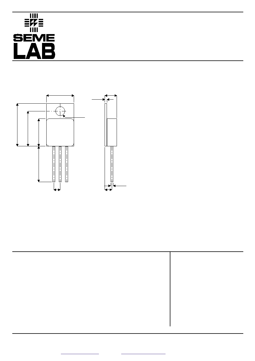
MECHANICAL DATA
Dimensions in mm (inches)
Dia.
2.65
2.75
0.89
1.14
0.70
0.90
4.70
5.00
10.41
10.67
3.56
3.81
16.
3
8
16.
8
9
13
.
3
9
13
.
6
4
10.
41
10.
92
12.
70
19.
05
2.54
BSC
1 2 3
P≠CHANNEL
MOS
TRANSISTOR
ABSOLUTE MAXIMUM RATINGS
(T
case
= 25∞C unless otherwise stated)
FEATURES
∑ P CHANNEL
∑ REPETITIVE AVALANCHE RATED
∑ DYNAMIC dv/dt RATING
∑ FAST SWITCHING
∑ EASE OF PARALLELING
∑ SIMPLE DRIVE REQUIREMENTS
V
DSS
≠50V
I
D(cont)
13.2A
R
DS(on)
0.15
W
W
W
W
TO≠220 ≠ Metal Package
Pin 1 ≠ Gate
Pin 2 ≠ Drain
Pin 3 ≠ Source
Parameter
Test Conditions
Min.
Typ.
Max.
Unit
-50
-0.060
0.15
-2
-4
3.1
-100
-500
-100
100
900
570
140
39
10
15
18
170
32
96
13.2
53
-6.3
120
250
0.47
1.1
4.5
7.5
SML9030≠220M
Prelim. 3/97
Semelab plc.
Telephone +44(0)1455 556565. Fax +44(0)1455 552612.
E-mail:
sales@semelab.co.uk
Website:
http://www.semelab.co.uk
V
GS
= 0
I
D
= -250
m
A
Reference to 25∞C
I
D
= -1mA
V
GS
= -10V
I
D
= 9.3A
V
DS
= V
GS
I
D
= -250
m
A
V
DS
= -40V
I
D
= 9.3A
V
DS
= -60V
V
GS
= 0
V
DS
= -48V
V
GS
= 0
T
J
= 125∞C
V
GS
= -20V
V
GS
= 20V
V
GS
= 0
V
DS
= -25V
f = 1MHz
I
D
= 13.2A
V
DS
= -48V
V
GS
= -10V
V
DD
= -30V
I
D
= 13.2A
R
G
= 12
W
R
D
= 1.5
W
I
S
= -18A
T
J
= 25∞C
V
GS
= 0
I
F
= -18A
T
J
= 25∞C
d
i
/ d
t
=
100A/
m
s
ELECTRICAL CHARACTERISTICS
(Tamb = 25∞C unless otherwise stated)
Drain ≠ Source Breakdown Voltage
Temperature Coefficient of
Breakdown Voltage
Static Drain ≠ Source On Resistance
1
Gate Threshold Voltage
Forward Transconductance
1
Zero Gate Voltage Drain Current
Forward Gate ≠ Source Leakage
Reverse Gate ≠ Source Leakage
Input Capacitance
Output Capacitance
Reverse Transfer Capacitance
Total Gate Charge
1
Gate ≠ Source Charge
1
Gate ≠ Drain ("Miller") Charge
1
Turn≠On Delay Time
1
Rise Time
1
Turn≠Off Delay Time
1
Fall Time
1
Continuous Source Current (Body Diode)
Pulse Source Current
2
(Body Diode)
Diode Forward Voltage
1
Reverse Recovery Time
1
Reverse Recovery Charge
1
V
V / ∞C
W
V
S
m
A
nA
pF
nC
nS
A
V
ns
m
C
nH
BV
DSS
D
BV
DSS
D
T
J
R
DS(on)
V
GS(th)
g
fs
I
DSS
I
GSS
I
GSS
C
iss
C
oss
C
rss
Q
g
Q
gs
Q
gd
t
d(on)
t
r
t
d(off)
t
f
I
S
I
SM
V
SD
t
rr
Q
rr
L
D
L
S
STATIC ELECTRICAL RATINGS
Notes
1) Pulse Test: Pulse Width
£
300ms,
d £
2%
2) Repetitive Rating ≠ Pulse width limited by maximum junction temperature.
DYNAMIC CHARACTERISTICS
SOURCE ≠ DRAIN DIODE CHARACTERISTICS
Internal Drain Inductance
(from 6mm down lead to centre of drain bond pad)
Internal Source Inductance
(from 6mm down lead to centre of source bond pad)
PACKAGE CHARACTERISTICS