SRF446
SRF447
Semelab plc.
Telephone +44(0)1455 556565. Fax +44(0)1455 552612. e-mail sales@semelab.co.uk
Website http://www.semelab.co.uk
Prelim. 5/98
DEVICE
SRF446
GATE
SOURCE
DRAIN
SRF447
DRAIN
SOURCE
GATE
V
DSS
V
DGO
I
D
V
GS
P
D
T
J
, T
STG
T
L
1
3
2
3.55 (0.140)
3.81 (0.150)
0.40 (0.016)
0.79 (0.031)
2.21 (0.087)
2.59 (0.102)
1.01 (0.040)
1.40 (0.055)
15.49 (0.610)
16.26 (0.640)
4.69 (0.185)
5.31 (0.209)
1.49 (0.059)
2.49 (0.098)
2
0
.8
0
(
0
.8
1
9
)
2
1
.4
6
(
0
.8
4
5
)
6.
15
(0
.
2
4
2
)
BS
C
19.
81 (
0
.
7
8
0
)
20.
32 (
0
.
8
0
0
)
4.
50
(
0
.
177)
Ma
x
.
1.65 (0.065)
2.13 (0.084)
5.25 (0.215)
B S C
2.87 (0.113)
3.12 (0.123)
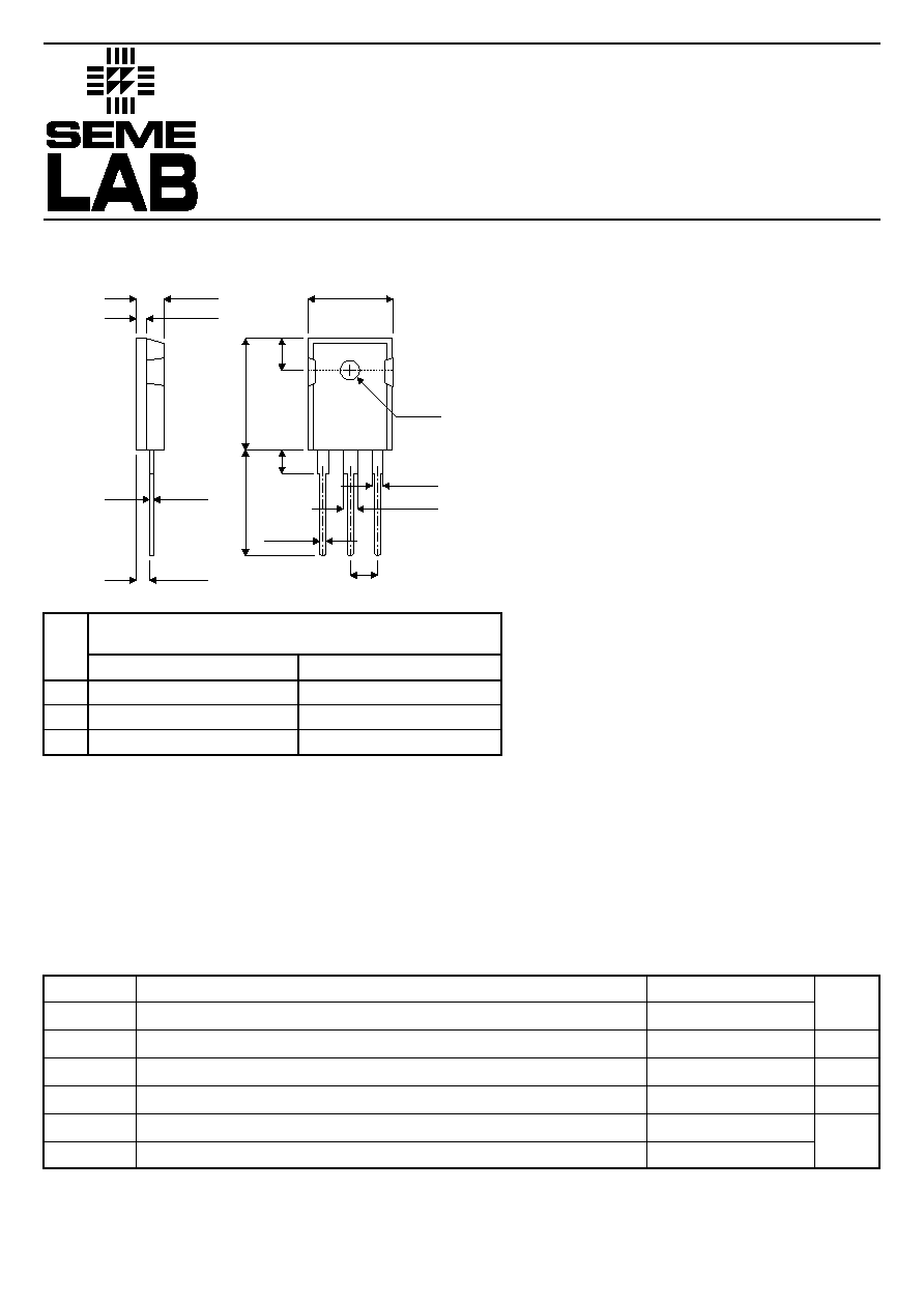
TO-247AD Package Outline.
Dimensions in mm (inches)
Drain ≠ Source Voltage
Drain ≠ Gate Voltage
Continuous Drain Current
Gate ≠ Source Voltage
Total Power Dissipation @ T
case
= 25∞C
Operating and Storage Junction Temperature Range
Lead Temperature : 0.063" from Case for 10 Sec.
N≠CHANNEL
ENHANCEMENT MODE
250W ≠ 250V ≠ 65MHz
900
900
6.5
±30
230
-55 to150
300
V
A
V
W
∞C
ABSOLUTE MAXIMUM RATINGS
(T
case
= 25∞C unless otherwise stated)
RF POWER MOSFET
FEATURES
∑
Low Cost Common Source RF
Package.
∑
Very High Breakdown for Improved
Ruggedness.
∑
Low Thermal Resistance.
∑
Nitride Passivated Die for Improved
Reliability.
PIN
NO
1
2
3
Dimensions in Millimeters and (Inches)
NOTE:
The SRF446 and SRF447 comprise a symmetric pair of RF Power
Transistors and meet the same electrical specifications. The
device pin-outs are the mirror image of each other to allow ease of
use as a push-pull pair.
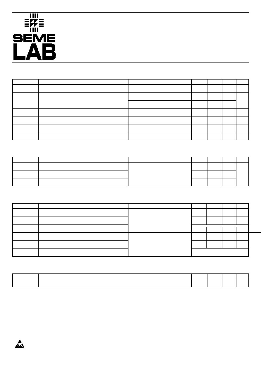
Characteristic
Test Conditions
Min.
Typ.
Max. Unit
Characteristic
Test Conditions
Min.
Typ.
Max. Unit
SRF446
SRF447
Semelab plc.
Telephone +44(0)1455 556565. Fax +44(0)1455 552612. e-mail sales@semelab.co.uk
Website http://www.semelab.co.uk
Prelim. 5/98
20
80
dB
%
No Degradation in Output
Power
1500
1800
70
130
27
50
C
iss
C
oss
C
rss
Characteristic
Min.
Typ.
Max. Unit
0.55
R
JC
Junction to Case
∞C/W
THERMAL CHARACTERISTICS
1) Pulse Test: Pulse Width < 380
µ
S , Duty Cycle < 2%
Input Capacitance
Output Capacitance
Reverse Transfer Capacitance
V
GS
= 0V
V
DS
= 300V
f = 1MHz
pF
CAUTION -- Electrostatic Sensitive Devices. Anti-Static Procedures Must Be Followed.
Characteristic
Test Conditions
Min.
Typ.
Max. Unit
BV
DSS
I
DSS
I
GSS
V
GS(TH)
g
fs
V
DS(ON)
V
GS
= 0V , I
D
= 250
µ
A
V
DS
= V
DSS
V
DS
= 0.8V
DSS
, T
C
= 125∞C
V
GS
= ±30V , V
DS
= 0V
V
DS
= V
GS
, I
D
= 50mA
V
DS
= 25V, I
D
= 3.5A
I
D(ON)
= 3.5A V
GS
= 10V
Drain ≠ Source Breakdown Voltage
Zero Gate Voltage Drain Current
(V
GS
= 0V)
Gate ≠ Source Leakage Current
Gate Threshold Voltage
Forward Transconductance
On State Drain Voltage
1
900
25
250
±100
2
5
4
5.7
7
V
µ
A
nA
V
S
V
STATIC ELECTRICAL RATINGS
(T
case
= 25∞C unless otherwise stated)
DYNAMIC CHARACTERISTICS
FUNCTIONAL CHARACTERISTICS
G
ps
G
ps
Common source Amplifier Power Gain
Drain Efficiency
Electrical Ruggedness VSWR 20:1
Common source Amplifier Power Gain
Drain Efficiency
Electrical Ruggedness VSWR 20:1
f = 27.12MHz
V
GS
= 0V
V
DD
= 300V
Pout = 250W
f = 40.68MHz
V
GS
= 0V
V
DD
= 250V
Pout = 250W
15
75
dB
%
No Degradation in Output
Power