
Type 2N3468L
Geometry 6706
Polarity PNP
Qual Level: JAN - JANTXV
Data Sheet No. 2N3468L
Generic Part Number:
2N3468
REF: MIL-PRF-19500/348
Features:
∑
General-purpose transistor for
switching and amplifier applica-
tons.
∑
Housed in a
TO-5
case.
∑
Also available in chip form using
the 6706 chip geometry.
∑
The Min and Max limits shown are
per
MIL-PRF-19500/348
which
Semicoa meets in all cases.
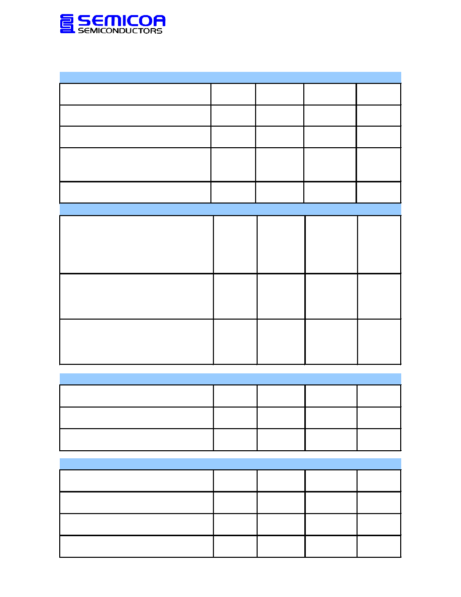
Rating Symbol Rating Unit
Collector-Emitter Voltage V
CEO
50 V
Collector-Base Voltage V
CBO
50 V
Emitter-Base Voltage V
EBO
5.0 V
Collector Current, Continuous I
C
1.0 mA
Operating Junction Temperature T
J
-55 to +175
o
C
Storage Temperature T
STG
-55 to +175
o
C
Maximum Ratings
T
C
= 25
o
C unless otherwise specified
TO-5
Data Sheet No. 2N3468L
OFF Characteristics
Symbol
Min
Max
Unit
Collector-Base Breakdown Voltage
I
C
= 10 µA
Collector-Emitter Breakdown Voltage
I
C
= 10 mA
Emitter-Base Breakdown Voltage
I
E
= 10 µA, pulsed
Collector-Base Cutoff Current
V
CB
= 30 V
I
CBO1
---
100
nA
V
CB
= 30 V, T
A
= +150
o
C
I
CBO2
---
50
µA
Collector-Emitter Cutoff Current
V
EB
= 3.0 V, V
CE
= 30 V
---
100
V
(BR)CEO
50
---
V
(BR)EBO
5.0
---
nA
V
Electrical Characteristics
T
C
= 25
o
C unless otherwise specified
V
V
V
(BR)CBO
50
---
I
CEX
ON Characteristics
Symbol
Min
Max
Unit
Forward current Transfer Ratio
I
C
= 150 mA, V
CE
= 1.0 V (pulse test)
h
FE1
25
---
---
I
C
= 500 mA, V
CE
= 1.0 V (pulse test)
h
FE2
25
75
---
I
C
= 1.0 A, V
CE
= 5 V (pulse test)
h
FE3
25
---
---
I
C
= 150 mA, V
CE
= 1.0 V (pulse test), T = -55
o
C
h
FE4
10
---
---
Collector-Emitter Saturation Voltage
I
C
= 150 mA, I
B
= 15 mA (pulse test)
V
CE(sat)1
---
0.35
V dc
I
C
= 500 mA, I
B
= 50 mA (pulse test)
V
CE(sat)2
---
0.6
V dc
I
C
= 1.0 A, I
B
= 100 mA (pulse test)
V
CE(sat)3
---
1.2
V dc
Base-Emitter Saturation Voltage
I
C
= 150 mA, I
B
= 15 mA (pulse test)
V
BE(sat)1
---
1.0
V dc
I
C
= 500 mA, I
B
= 50 mA (pulse test)
V
BE(sat)2
0.8
1.2
V dc
I
C
= 1.0 A, I
B
= 100 mA (pulse test)
V
BE(sat)3
---
1.6
V dc
Small Signal Characteristics
Symbol
Min
Max
Unit
Extrapolated Unity Gain Frequency
V
CE
= 10 V, I
C
= 50 mA, f = 100 MHz
Open Circuit Output Capacitance
V
CB
= 10 V, I
E
= 0, 100 kHz < f < 1 MHz
Input Capacitance, Output Open Circuited
V
EB
= 0.5 V, I
C
= 0, 100 kHz < f < 1 MHz
C
IBO
---
100
pF
pF
C
OBO
---
25
MHz
f
t
150
500
Switching Characteristics
Symbol
Min
Max
Unit
Delay Time
I
C
= 500 mA, I
B1
= 50 mA, V
EB
= 2 V
Rise Time
I
C
= 500 mA, I
B1
= 50 mA, V
EB
= 2 V
Storage Time
I
C
= 500 mA, I
B1
= I
B2
= 50 mA
Fall Time
I
C
= 500 mA, I
B1
= I
B2
= 50 mA
ns
t
d
---
10
t
r
---
30
ns
t
s
---
60
ns
t
f
---
30
ns