October 2000
Copyright ©2000 Alliance Semiconductor. All rights reserved.
®
AS6UA5128
10/6/00
ALLIANCE SEMICONDUCTOR
1
2.3V to 3.6V 512K×8 Intelliwatt low-power CMOS SRAM
Features
· AS6UA5128
· IntelliwattTM active power circuitry
· Industrial and commercial temperature ranges available
· Organization: 524,288 words × 8 bits
· 2.7V to 3.6V at 55 ns
· 2.3V to 2.7V at 70 ns
· Low power consumption: ACTIVE
- 144 mW at 3.6V and 55 ns
- 68 mW at 2.7V and 70 ns
· Low power consumption: STANDBY
- 72 µW max at 3.6V
- 41 µW max at 2.7V
- 28 µW max at 2.3V
· 1.2V data retention
· Equal access and cycle times
· Easy memory expansion with CS, OE inputs
· Smallest footprint packages
- 36(48)-ball FBGA
- 32-pin TSOP I and TSOP II packages are available on
Alliance AS6UB5128 product family (available January
2001)
· ESD protection
2000 volts
· Latch-up current
200 mA
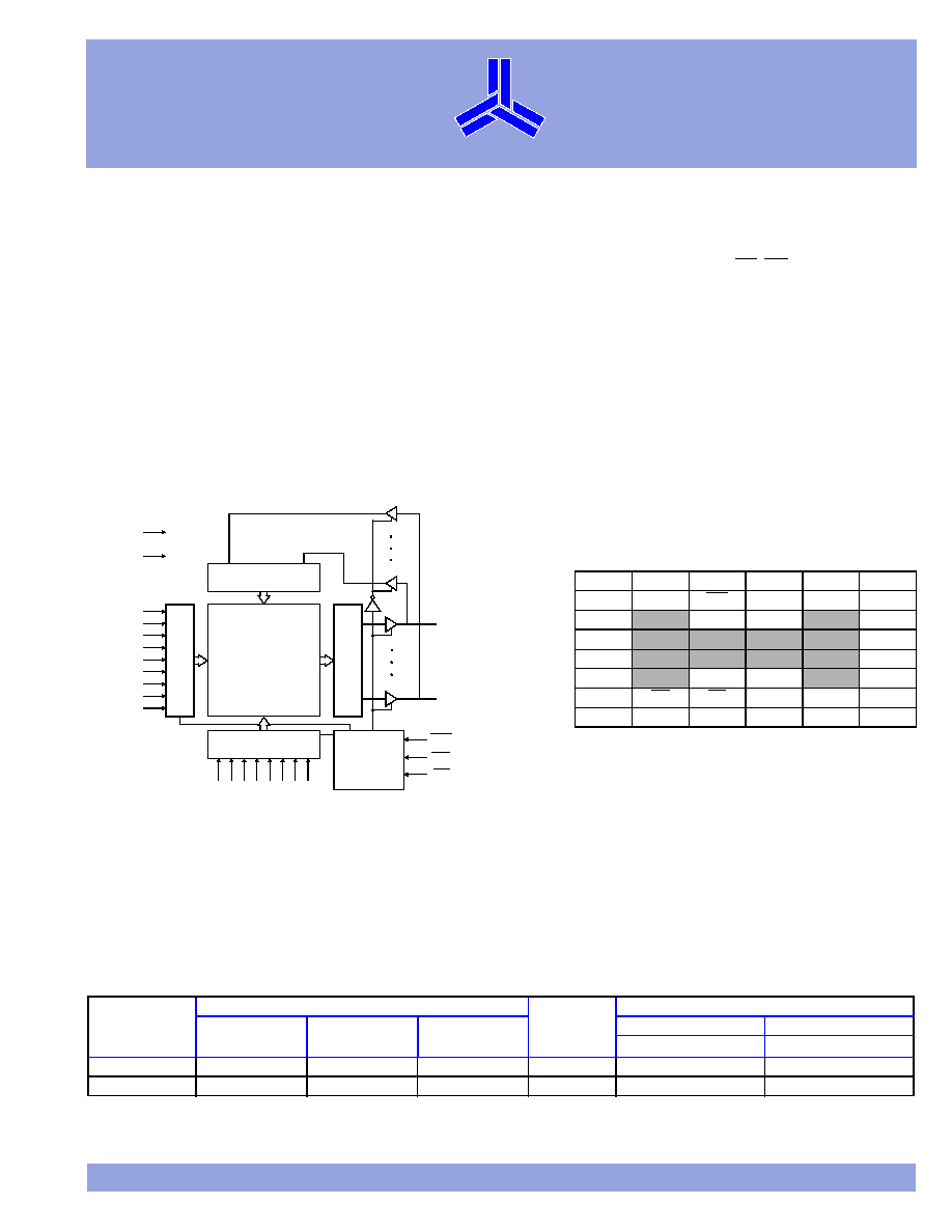
Logic block diagram
Se
ns
e am
p
Input buffer
A1
0
A1
1
A1
2
A1
3
A1
4
A1
5
A1
6
I/O1
I/O8
OE
CS
WE
Row
de
co
de
r
Control
circuit
A9
A0
A1
A2
A3
A4
A5
A6
A7
V
CC
GND
A8
Column decoder
512K
×
8
Array
(4,194,304)
Pin arrangement
36(48)-CSP BGA Package
(shading indicates no ball)
1
2
3
4
5
6
A
A
0
A
1
NC
A
3
A
6
A
8
B
I/O5
A
2
WE
A
4
A
7
I/O
1
C
I/O6
NC
A
5
I/O
2
D
V
SS
V
CC
E
V
CC
V
SS
F
I/O7
A
18
A
17
I/O3
G
I/O8
OE
CS
A
16
A
15
I/O4
H
A
9
A
10
A
11
A
12
A
13
A
14
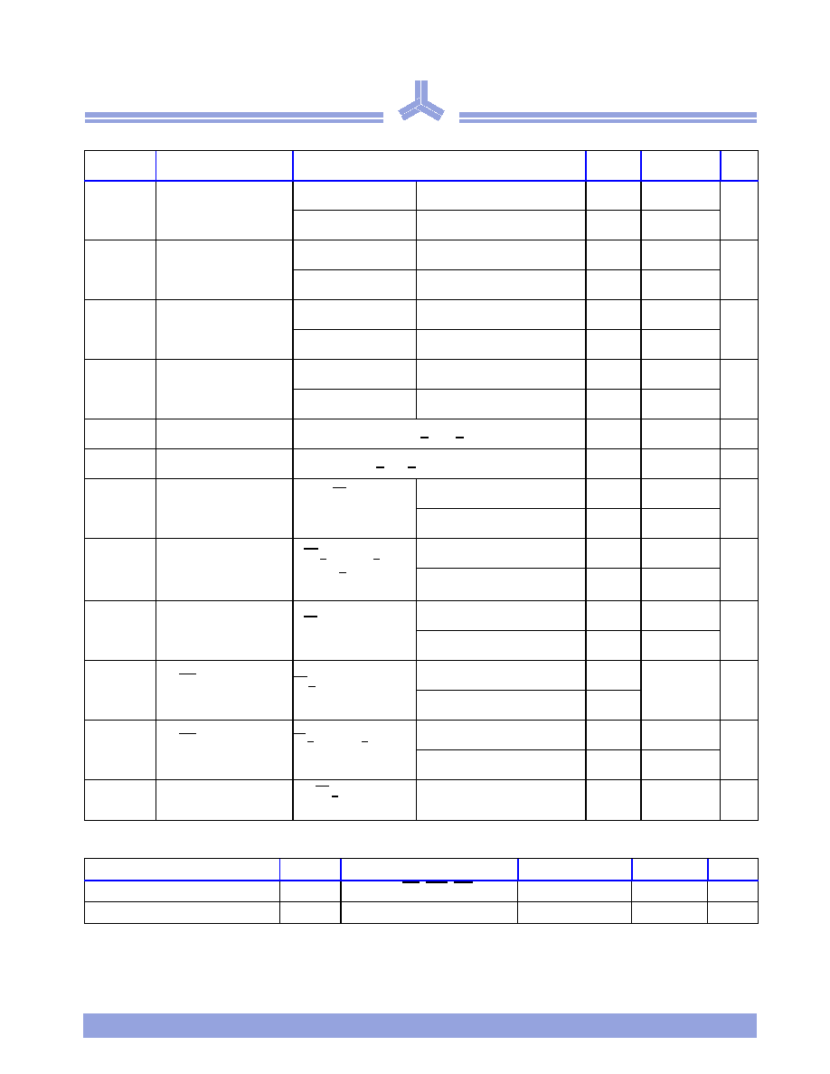
Selection guide
Product
V
CC
Range
Speed
(ns)
Power Dissipation
Min
(V)
Typ
2
(V)
Max
(V)
Operating (I
CC
)
Standby (I
SB1
)
Max (mA)
Max (
µ
µ
µ
µ
A)
AS6UA5128
2.7
3.0
3.6
55
2
20
AS6UA5128
2.3
2.5
2.7
70
1
15
®
2
ALLIANCE SEMICONDUCTOR
10/6/00
AS6UA5128
Functional description
The AS6UA5128 is a low-power CMOS 4,194,304-bit Static Random Access Memory (SRAM) device organized as
524,288 words × 8 bits. It is designed for memory applications where slow data access, low power, and simple interfacing
are desired.
Equal address access and cycle times (t
AA
, t
RC
, t
WC
) of 55/70ns are ideal for low-power applications. Active high and low
chip selects (CS) permit easy memory expansion with multiple-bank memory systems.
When CS is high, the device enters standby mode: the AS6UA5128 is guaranteed not to exceed 72
µ
W power consumption
at 3.6V and 55 ns; 41
µ
W at 2.7V and 70 ns; or 28
µ
W at 2.3V and 100 ns. The device also returns data when V
CC
is
reduced to 1.5V for even lower power consumption.
A write cycle is accomplished by asserting write enable ( WE) and chip select (CS) low. Data on the input pins I/O1I/O8 is
written on the rising edge of WE (write cycle 1) or CS (write cycle 2). To avoid bus contention, external devices should drive
I/O pins only after outputs have been disabled with output enable (OE) or write enable (WE).
A read cycle is accomplished by asserting output enable (OE), chip select (CS), with write enable (WE) High. The chip
drives I/O pins with the data word referenced by the input address. When either chip select or output enable is inactive, or
write enable is active, output drivers stay in high-impedance mode.
All chip inputs and outputs are CMOS-compatible, and operation is from a single 2.3V to 3.6V supply. The device is
available in the JEDEC standard 36(48)-ball FBGA package.
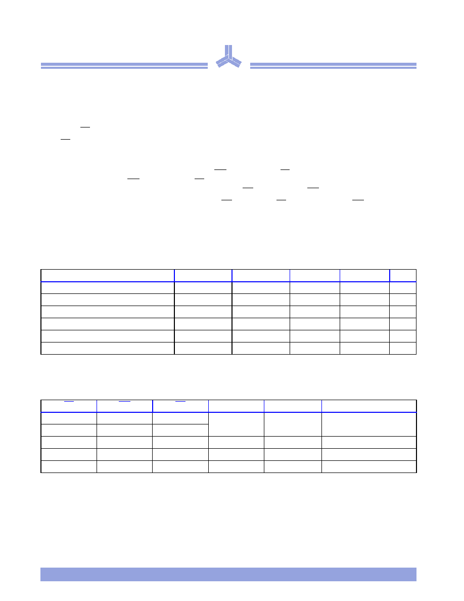
Absolute maximum ratings
Note: Stresses greater than those listed under Absolute Maximum Ratings may cause permanent damage to the device. This is a stress rating only and func-
tional operation of the device at these or any other conditions outside those indicated in the operational sections of this spec ification is not implied. Expo-
sure to absolute maximum rating conditions for extended periods may affect reliability.
Truth table
Key: X = Don't care, L = Low, H = High.
Parameter
Device
Symbol
Min
Max
Unit
Voltage on V
CC
relative to V
SS
V
tIN
0.5
V
CC
+ 0.5
V
Voltage on any I/O pin relative to GND
V
tI/O
0.5
V
Power dissipation
P
D
1.0
W
Storage temperature (plastic)
T
stg
65
+150
°
C
Temperature with V
CC
applied
T
bias
55
+125
°
C
DC output current (low)
I
OUT
20
mA
CS
WE
OE
Supply Current
I/O1I/O8
Mode
H
X
X
I
SB
High Z
Standby (I
SB
)
L
X
X
L
H
H
I
CC
High Z
Output disable (I
CC
)
L
H
L
I
CC
D
OUT
Read (I
CC
)
L
L
X
I
CC
D
IN
Write (I
CC
)
®
4
ALLIANCE SEMICONDUCTOR
10/6/00
AS6UA5128
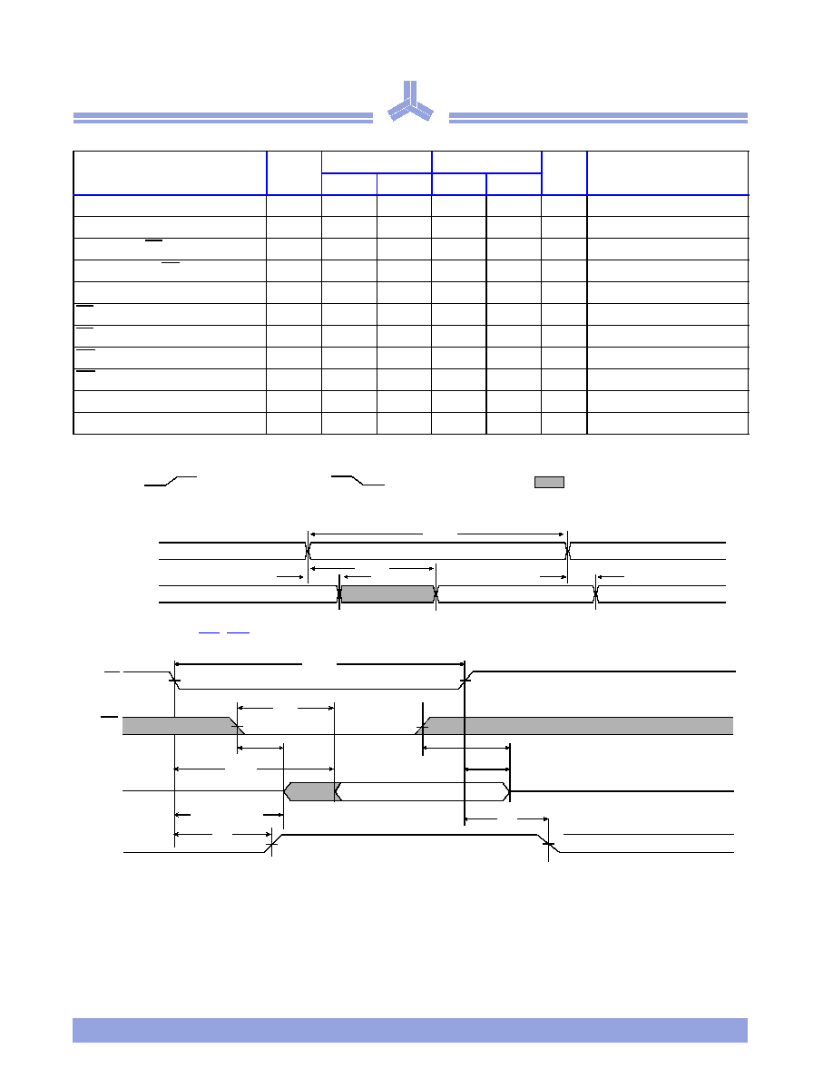
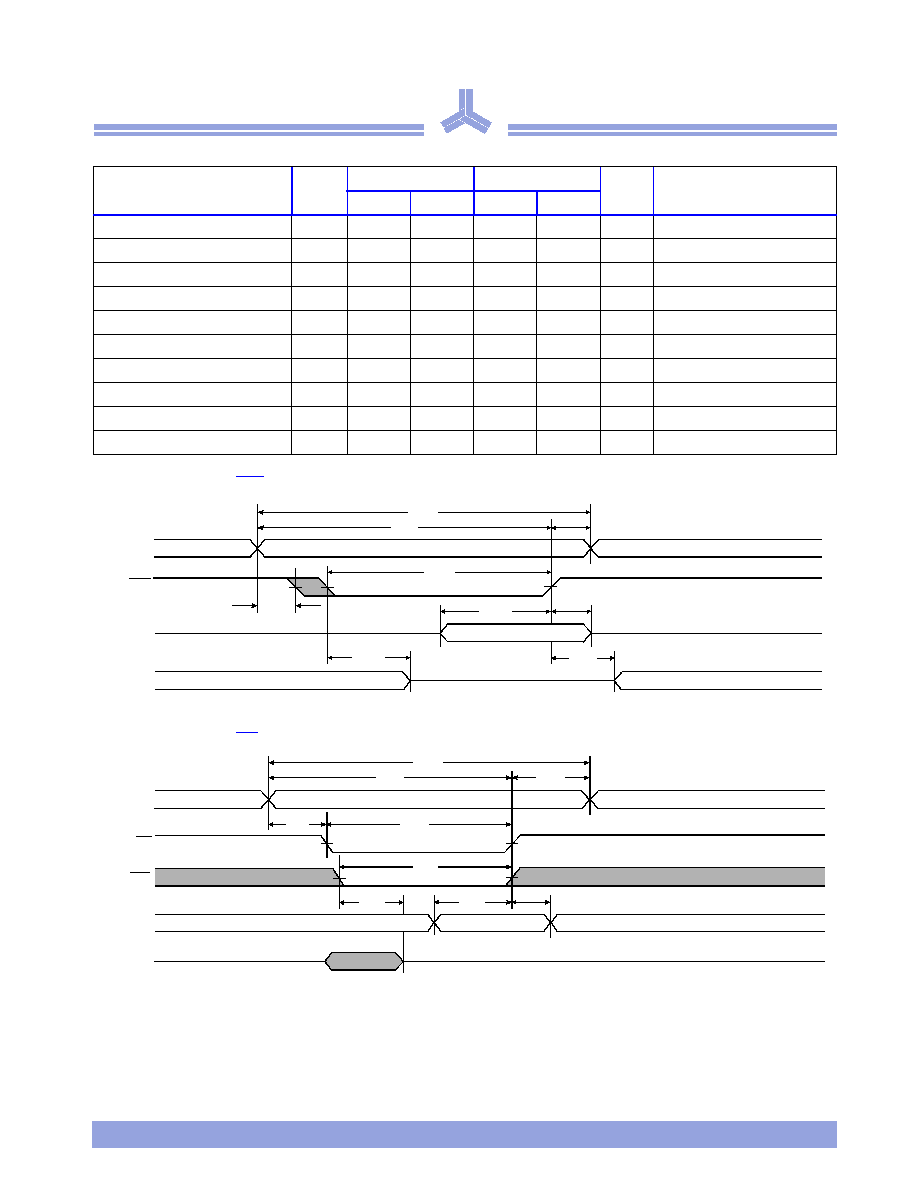
Read cycle (over the operating range)
3,9
Key to switching waveforms
Read waveform 1 (address controlled)
3,6,7,9
Read waveform 2 (CS, OE controlled)
3,6,8,9
Parameter
Symbol
55
70
Unit
Notes
Min
Max
Min
Max
Read cycle time
t
RC
55
70
ns
Address access time
t
AA
55
70
ns
3
Chip select (CS) access time
t
ACS
55
70
ns
3
Output enable (OE) access time
t
OE
25
35
ns
Output hold from address change
t
OH
10
10
ns
5
CS low to output in low Z
t
CLZ
10
10
ns
4, 5
CS high to output in high Z
t
CHZ
0
20
0
20
ns
4, 5
OE low to output in low Z
t
OLZ
5
5
ns
4, 5
OE high to output in high Z
t
OHZ
0
20
0
20
ns
4, 5
Power up time
t
PU
0
0
ns
4, 5
Power down time
t
PD
55
S
70
ns
S
Undefined/don't care
Falling input
Rising input
t
OH
t
AA
t
RC
t
OH
D
OUT
Address
Data valid
Previous data valid
current
Supply
OE
D
OUT
t
OE
t
OLZ
t
ACE
t
CHZ
t
CLZ
t
PU
t
PD
I
CC
I
SB
50%
50%
t
OHZ
Data valid
t
RC1
CS
®
AS6UA5128
10/6/00
ALLIANCE SEMICONDUCTOR
5
Write cycle (over the operating range)
11
Write waveform 1 (WE controlled)
10,11
Write waveform 2 (CS controlled)
10,11
Parameter
Symbol
55
70
Unit
Notes
Min
Max
Min
Max
Write cycle time
t
WC
55
70
ns
Chip select to write end
t
CW
40
60
ns
12
Address setup to write end
t
AW
40
60
ns
Address setup time
t
AS
0
0
ns
12
Write pulse width
t
WP
35
55
ns
Address hold from end of write
t
AH
0
0
ns
Data valid to write end
t
DW
25
30
ns
Data hold time
t
DH
0
0
ns
4, 5
Write enable to output in high Z
t
WZ
0
20
0
20
ns
4, 5
Output active from write end
t
OW
5
5
ns
4, 5
t
AW
t
AH
t
WC
Address
WE
D
OUT
t
DH
t
OW
t
DW
t
WZ
t
WP
t
AS
Data valid
D
IN
t
AW
Address
CS
WE
D
OUT
t
CW
t
WP
t
DW
t
DH
t
AH
t
WZ
t
WC
t
AS
Data valid
D
IN