 | –≠–ª–µ–∫—Ç—Ä–æ–Ω–Ω—ã–π –∫–æ–º–ø–æ–Ω–µ–Ω—Ç: L6100200 | –°–∫–∞—á–∞—Ç—å:  PDF PDF  ZIP ZIP |
SKYPERTM 32PRO -
Technical Explanations
1 / 16
2005-06-03 ≠ Rev02
© by SEMIKRON
SKYPERTM 32PRO
Technical Explanations
Revision 02
Status: preliminary
--------------------------------------------------------------------------------------------------------------------------------------------------------------------------
This Technical Explanation is valid for the following parts:
part number
type
date code (YYWW)
L6100200 SKYPERTM
32PRO
0520
Related documents:
title version
Data Sheet SKYPERTM 32PRO
03-06-2005
Prepared by: Markus Hermwille
--------------------------------------------------------------------------------------------------------------------------------------------------------------------------
Content
Application and Handling Instructions...................................................................................................................... 2
Further application support...................................................................................................................................... 2
General Description................................................................................................................................................. 2
Features of SKYPERTM 32PRO............................................................................................................................... 2
Block diagram.......................................................................................................................................................... 3
Dimensions.............................................................................................................................................................. 3
PIN Array ≠ Primary Side......................................................................................................................................... 4
PIN Array ≠ Secondary Side.................................................................................................................................... 5
Driver Performance ................................................................................................................................................. 6
Insulation ................................................................................................................................................................. 6
Auxiliary Power Supply............................................................................................................................................ 6
Under Voltage Reset (UVR) .................................................................................................................................... 7
Under Voltage Protection (UVP) primary................................................................................................................. 8
Under Voltage Protection secondary ....................................................................................................................... 8
Input Signals............................................................................................................................................................ 8
Short Pulse Suppression (SPS)............................................................................................................................... 9
Failure Management................................................................................................................................................ 9
Halt Logic Signal (HLS) ........................................................................................................................................... 9
Dead Time generation (Interlock TOP / BOT) adjustable (DT) .............................................................................. 10
Dynamic Short Circuit Protection by V
CEsat
monitoring / de-saturation monitoring (DSCP).................................... 11
Adjustment of DSCP.............................................................................................................................................. 12
High Voltage Diode for DSCP................................................................................................................................ 12
Gate resistors ........................................................................................................................................................ 13
Soft Turn-Off (STO) ............................................................................................................................................... 13
External Error Input (EEI) ...................................................................................................................................... 14
Application Example .............................................................................................................................................. 14
Mounting Notes ..................................................................................................................................................... 15
Marking.................................................................................................................................................................. 16
Information furnished in this document is believed to be accurate and reliable. However, no representation or warranty is
given and no liability is assumed with respect to the accuracy or use of such information. Furthermore, this technical
information specifies semiconductor devices but promises no characteristics. No warranty or guarantee expressed or
implied is made regarding delivery, performance or suitability. Specifications mentioned in this document are subject to
change without notice. This document supersedes and replaces all information previously supplied and may be supersede
by updates.

SKYPERTM 32PRO -
Technical Explanations
2 / 16
2005-06-03 ≠ Rev02
© by SEMIKRON
SKYPERTM 32PRO
Application and Handling Instructions
Please provide for static discharge protection during handling. As long as the hybrid driver is not completely
assembled, the input terminals have to be short-circuited. Persons working with devices have to wear a
grounded bracelet. Any synthetic floor coverings must not be statically chargeable. Even during
transportation the input terminals have to be short-circuited using, for example, conductive rubber.
Worktables have to be grounded. The same safety requirements apply to MOSFET- and IGBT-modules.
Any parasitic inductances within the DC-link have to be minimised. Over-voltages may be absorbed by C- or
RCD-snubbers between main terminals for PLUS and MINUS of the power module.
When first operating a newly developed circuit, SEMIKRON recommends to apply low collector voltage and
load current in the beginning and to increase these values gradually, observing the turn-off behaviour of the
free-wheeling diode and the turn-off voltage spikes generated across the IGBT. An oscillographic control will
be necessary. Additionally, the case temperature of the module has to be monitored. When the circuit works
correctly under rated operation conditions, short-circuit testing may be done, starting again with low collector
voltage.
It is important to feed any errors back to the control circuit and to switch off the device immediately in failure
events. Repeated turn-on of the IGBT into a short circuit with a high frequency may destroy the device.
The inputs of the hybrid driver are sensitive to over-voltage. Voltages higher than V
S
+0,3V or below -0,3V
may destroy these inputs. Therefore, control signal over-voltages exceeding the above values have to be
avoided.
The connecting leads between hybrid driver and the power module should be as short as possible (max.
20cm), the driver leads should be twisted.
Further application support
Latest information is available at
http://www.semikron.com
. For design support please read the SEMIKRON
Application Manual Power Modules available at
http://www.semikron.com
.
General Description
The SKYPERTM 32PRO core constitutes an interface between IGBT modules and the controller. This core is a
half bridge driver. Functions for driving, potential separation and protection are integrated in the driver. Thus it can
be used to build up a driver solution for IGBT modules.
Features of SKYPERTM 32PRO
Two
output
channels
Integrated potential free power supply for secondary side
Short Pulse Suppression (SPS)
Under Voltage Protection (UVP) primary & secondary
Under Voltage Reset (UVR)
Drive interlock (dead time) top / bottom (DT) adjustable
Dynamic Short Circuit Protection (DSCP) by V
CE
monitoring and
direct switch off
Soft Turn-Off (STO)
Halt Logic Signal (HLS)
Failure
Management
External
Error
Input
DC bus voltage up to 1200V
Coated with varnish
Please note:
All values in this technical explanation are typical values. Typical values are the average values expected in large
quantities and are provided for information purposes only. These values can and do vary in different applications. All
operating parameters should be validated by user's technical experts for each application.

SKYPERTM 32PRO -
Technical Explanations
3 / 16
2005-06-03 ≠ Rev02
© by SEMIKRON
Block diagram
Block diagram
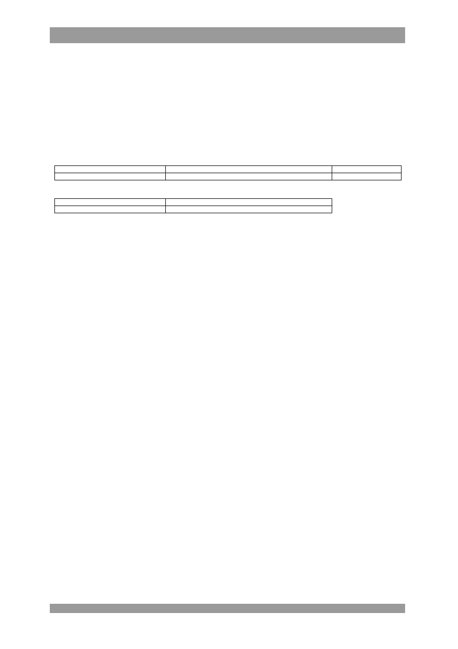
Dimensions
Dimensions in mm

SKYPERTM 32PRO -
Technical Explanations
4 / 16
2005-06-03 ≠ Rev02
© by SEMIKRON
PIN Array ≠ Primary Side
Connectors
Connector X10 / X11 (RM2,54, 10pin)
2,54
SQ 0,64
PIN
Signal
Function
Specification
X10:01 PRIM_nPWRFAIL_IN
Under Voltage Reset (supervisor
reset to be driven by an external
circuitry)
Inverted 15 V logic; 100kOhm
impedance; LOW = hold; HIGH =
normal operation
X10:02 reserved
X10:03
PRIM_HALT_OUT
Driver core status output
Digital 15 V logic; 100kOhm
impedance; LOW = ready to operate;
HIGH = not ready to operate
X10:04
PRIM_HALT_IN
Driver core status input
Digital 15 V logic; 100kOhm
impedance; LOW = enable driver; HIGH
= disable driver
X10:05 PRIM_PWR_GND
GND for power supply and GND for
digital signals
X10:06 PRIM_PWR_GND
GND for power supply and GND for
digital signals
X10:07
PRIM_TOP_IN
Switching signal input (TOP switch)
Digital 15 V logic; 100kOhm
impedance; LOW = TOP switch off;
HIGH = TOP switch on
X10:08 PRIM_BOT_IN
Switching signal input (BOTTOM
switch)
Digital 15 V logic; 100kOhm
impedance; LOW = BOT switch off;
HIGH = BOT switch on
X10:09
PRIM_PWR_15P
Drive core power supply
Stabilised +15V ±4%
X10:10
PRIM_PWR_15P
Drive core power supply
Stabilised +15V ±4%
X11:01 reserved
X11:02 reserved
X11:03 PRIM_PWR_GND
GND for power supply and GND for
digital signals
X11:04 PRIM_PWR_GND
GND for power supply and GND for
digital signals
X11:05
PRIM_CFG_TDT2_IN
Digital adjustment of locking time
Dead time bit #2
X11:06 PRIM_CFG_SELECT_IN
Signal for neutralizing locking
function
X11:07
PRIM_CFG_TDT3_IN
Digital adjustment of locking time
Dead time bit #3
X11:08
PRIM_CFG_TDT1_IN
Digital adjustment of locking time
Dead time bit #1
X11:09 PRIM_PWR_GND
GND for power supply and GND for
digital signals
X11:10 PRIM_PWR_GND
GND for power supply and GND for
digital signals
SKYPERTM 32PRO -
Technical Explanations
5 / 16
2005-06-03 ≠ Rev02
© by SEMIKRON
PIN Array ≠ Secondary Side
Connectors
Connector X100 / X200 (RM2,54, 10pin)
2,54
SQ 0,64
PIN
Signal
Function
Specification
X100:01
SEC_TOP_VCE_CFG
Input reference voltage adjustment
X100:02 SEC_TOP_VCE_IN
Input
V
CE
monitoring
X100:03
SEC_TOP_15P
Output power supply
Stabilised +15V / max. 10mA
1)
X100:04
SEC_TOP_ERR_IN
External error input
Voltage input; 6,6kOhm impedance;
LOW = ERROR
X100:05
SEC_TOP_IGBT_ON
Switch on signal TOP IGBT
X100:06
SEC_TOP_IGBT_OFF
Switch off signal TOP IGBT
X100:07 SEC_TOP_GND
GND for power supply and GND for
digital signals
X100:08 SEC_TOP_GND
GND for power supply and GND for
digital signals
X100:09 SEC_TOP_IGBT_SOFTOFF
Control input for setting soft turn-off
TOP IGBT
X100:10
SEC_TOP_8N
Output power supply
Stabilised -7V / max. 10mA
1)
X200:01
SEC_BOT_VCE_CFG
Input reference voltage adjustment
X200:02
SEC_ BOT_VCE_IN
Input V
CE
monitoring
X200:03
SEC_ BOT_15P
Output power supply
Stabilised +15V / max. 10mA
1)
X200:04
SEC_ BOT_ERR_IN
External error input
Voltage input; 6,6kOhm impedance;
LOW = ERROR
X200:05
SEC_ BOT_IGBT_ON
Switch on signal BOT IGBT
X200:06
SEC_ BOT_IGBT_OFF
Switch off signal BOT IGBT
X200:07 SEC_
BOT_GND
GND for power supply and GND for
digital signals
X200:08 SEC_
BOT_GND
GND for power supply and GND for
digital signals
X200:09 SEC_BOT_IGBT_SOFTOFF
Control input for setting soft turn-off
BOT IGBT
X200:10
SEC_BOT_8N
Output power supply
Stabilised -7V / max. 10mA
1)
1)
The average output current of the driver will be reduced accordingly.

SKYPERTM 32PRO -
Technical Explanations
6 / 16
2005-06-03 ≠ Rev02
© by SEMIKRON
Driver Performance
The driver is designed for application with half bridges or single modules and a maximum gate charge per pulse
< 6,3µC. The charge necessary to switch the IGBT is mainly depending on the IGBT's chip size, the DC-link
voltage and the gate voltage. This correlation is shown in module datasheets. It should, however, be considered
that the driver is turned on at +15V and turned off at -7V. Therefore, the gate voltage will change by 22V during
each switching procedure. Unfortunately, many datasheets do not show negative gate voltages. In order to
determine the required charge, the upper leg of the charge curve may be prolonged to +22V for determination of
approximate charge per switch.
The medium output current of the driver is determined by the switching frequency and the gate charge. The
maximum switching frequency may be calculated with the shown equations.
Calculation Switching Frequency
Maximum Switching Frequency @ different Gate Charges @ T
amb
=25∞C
f
max
: Maximum switching frequency
Iout
AVmax
: Maximum output average current
Q
GE
: Gate charge of the driven IGBT
0 kHz
10 kHz
20 kHz
30 kHz
40 kHz
50 kHz
60 kHz
0 µC
1 µC
2 µC
3 µC
4 µC
5 µC
6 µC
7 µC
gate charge
s
w
itc
h
ing fr
e
que
nc
y
Insulation
Magnetic transformers are used for insulation between gate driver primary and secondary side. The transformer
set consists of pulse transformers which are used bidirectional for turn-on and turn-off signals of the IGBT and the
error feedback between secondary and primary side, and a DC/DC converter. This converter provides a potential
separation (galvanic separation) and power supply for the two secondary (TOP and BOT) sides of the driver.
Thus, external transformers for power supply are not required.
Creepage and Clearance Distance in mm
Primary to secondary
Min. 12,2
Auxiliary Power Supply
A few basic rules should be followed when dimensioning the customer side power supply for the driver. The
following table shows the required features of an appropriate power supply.
Requirements of the auxiliary power supply
Regulated power supply
+15V ±4%
Maximum rise time of auxiliary power supply
50ms
Minimum peak current of auxiliary supply
1A
Power on reset completed after
150ms
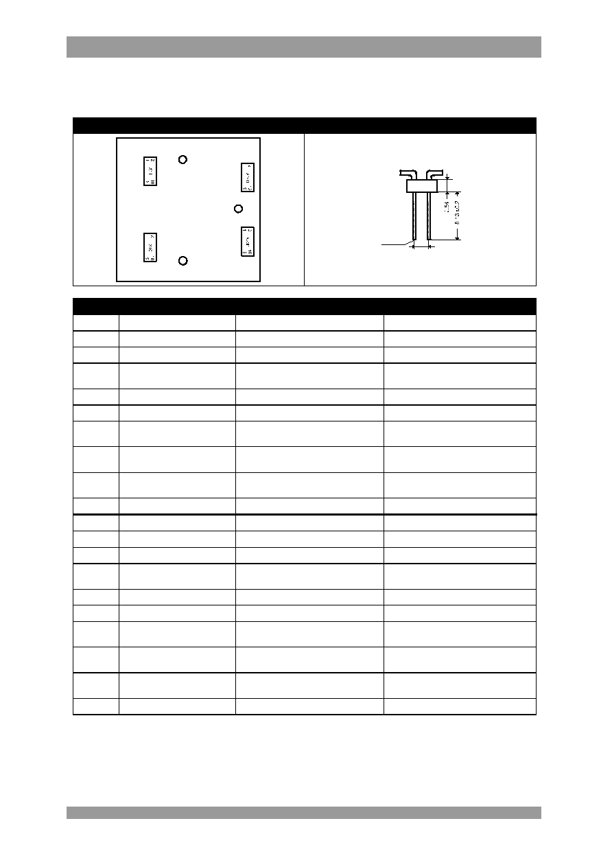
The supplying switched mode power supply may not be turned-off for a short time as consequence of its current
limitation. Its output characteristic needs to be considered. Switched mode power supplies with fold-back
Please note:
Do not apply switching
signals during power on
reset.
Please note:
The maximum value of the switching frequency is limited to 50kHz due to switching reasons.
GE
max
AV
max
Q
Iout
f
=
SKYPERTM 32PRO -
Technical Explanations
7 / 16
2005-06-03 ≠ Rev02
© by SEMIKRON
characteristic or hiccup-mode can create problems if no sufficient over current margin is available. The voltage
has to rise continuously and without any plateau formation as shown in the following diagram.
Rising slope of the power supply voltage
If the power supply is able to provide a higher current, a peak current will flow in the first instant to charge up the
input capacitances on the driver. Its peak current value will be limited by the power supply and the effective
impedances (e.g. distribution lines), only.
It is recommended to avoid the paralleling of several customer side power supply units. Their different set current
limitations may lead to dips in the supply voltage.
The driver is ready for operation typically 150ms after turning on the supply voltage. The driver error signal
PRIM_HOLD_OUT and PRIM_HOLD_IN are operational after this time. Without any error present, the
PRIM_HOLD_OUT signal will be reset.
To assure a high level of system safety the TOP and BOT signal inputs should stay in a defined state (OFF state,
LOW) during driver turn-on time. Only after the end of the power-on-reset, IGBT switching operation shall be
permitted.
Under Voltage Reset (UVR)
The Under Voltage Reset circuit configures the driver core to hold in a reset state during power on and power off.
UVR can be thought of as a supplement function to the build in power-on-reset by the user. While in reset, the
driver is held in its initial condition until PRIM_nPWRFAIL_IN is forced into HIGH state. Once the system reset
sequence completes, the driver core is ready to operate.
UVR input
Application Hints
A capacitor is connected to the input to obtain high noise
immunity.
Disabling of the Under Voltage Reset function
(PRIM_nPWRFAIL_IN) can be achieved by no
connection or connection to +15V.
Please note:
Do not use PRIM_nPWRFAIL_IN to place the driver core into halt mode during operation.

SKYPERTM 32PRO -
Technical Explanations
8 / 16
2005-06-03 ≠ Rev02
© by SEMIKRON
Under Voltage Protection (UVP) primary
The internally detected supply voltage of the driver has an under voltage protection. The table below gives an
overview of the trip level.
Supply voltage
UVP level
Regulated +15V ±4%
13,5V
If the internally detected supply voltage of the driver falls below this level, the IGBTs will be switched off (IGBT
driving signals set to LOW). The input side switching signals of the driver will be ignored. The error memory will
be set, and the output PRIM_HOLD_OUT changes to the HIGH state.
Under Voltage Protection secondary
This function monitors the rectified voltage on the secondary side. If the voltage drops, the IGBTs will be switched
off (IGBT driving signal set to LOW). The input side switching signals of the driver will be ignored. No failure
message will be generated.
Output voltage
UVP level
Regulated +15V
12V
Input Signals
The signal transfer to each IGBT is made with pulse transformers, used for switching on and switching off of the
IGBT. The inputs have a Schmitt Trigger characteristic and a positive / active high logic (input HIGH = IGBT on;
input LOW = IGBT off).
It is mandatory to use circuits which switch active to +15V and 0V. Pull up and open collector output stages must
not be used for TOP / BOT control signals. It is recommended choosing the line drivers according to the
demanded length of the signal wires.
TOP / BOT Input
A capacitor is connected to the input to obtain high noise
immunity. This capacitor can cause for current limited line
drivers a little delay of few ns, which can be neglected. The
capacitors have to be placed as close as possible to the
driver interface.
Please note:
It is not permitted to apply switching pulses shorter than 1µs.
SKYPERTM 32PRO -
Technical Explanations
9 / 16
2005-06-03 ≠ Rev02
© by SEMIKRON
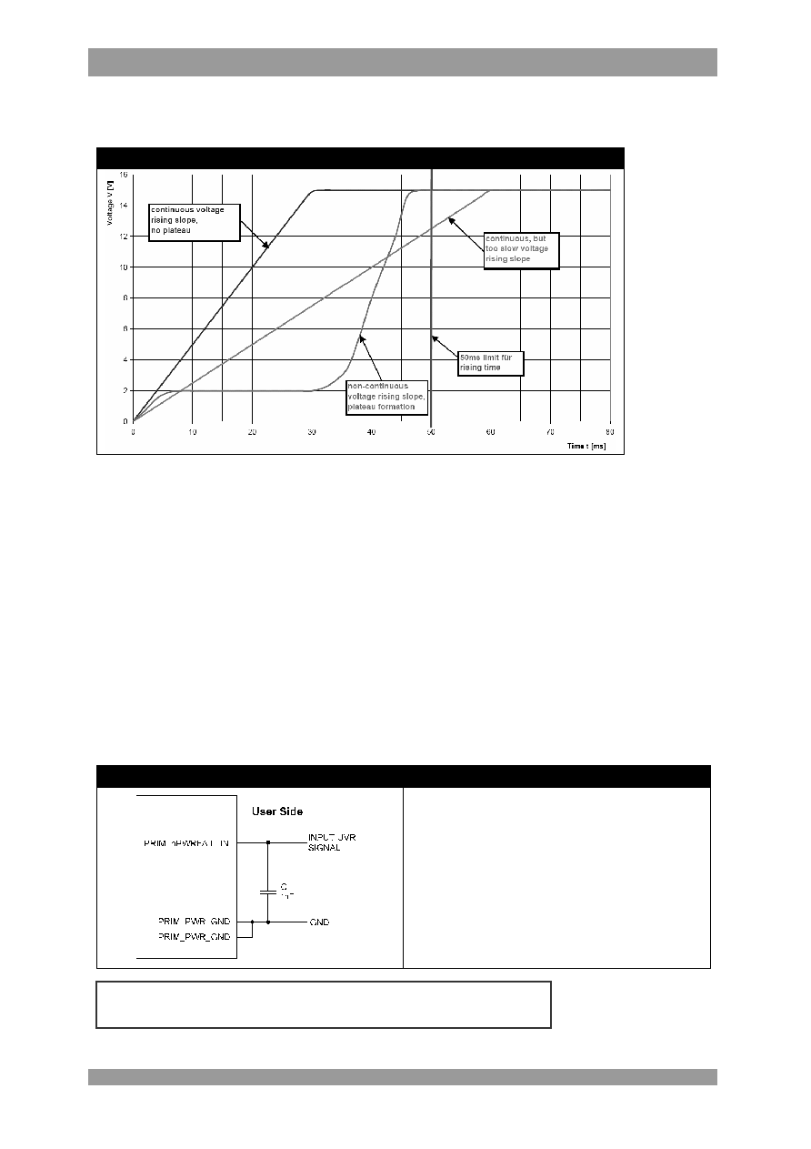
Short Pulse Suppression (SPS)
This circuit suppresses short turn-on and off-pulses of incoming signals. This way the IGBTs are protected
against spurious noise as they can occur due to bursts on the signal lines. Pulses shorter than 625ns are
suppressed and all pulses longer than 750ns get through for 100% probability. Pulses with a length in-between
625ns and 750ns can be either suppressed or get through.
Pulse pattern ≠ SPS
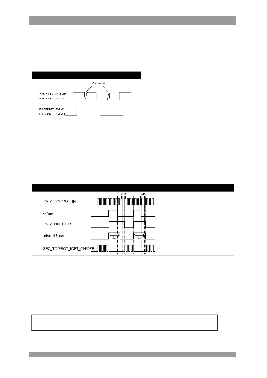
Failure Management
A failure caused by PRIM_nPWRFAIL_IN, under voltage protection, dynamic short circuit detection or external
error input will force PRIM_HALT_OUT into HIGH state (not ready to operate). The IGBTs will be switched off
(IGBT driving signals set to LOW) and switching pulses from the controller will be not transferred to the output
stage. At the same time an internal timer with a time constant of 3s is started. If no failure is present anymore, a
time of 3s after failure detection is passed and also TOP and BOT input signals are set to the LOW level for a
period of minimum t
pERRRESET
> 9µs, the driver core is ready to operate and switching pulse are transferred to the
output stage.
Pulse Pattern Failure Management
Propagation delay of the driver,
interlock dead time and switching time
of the IGBT chip has to be taken into
account (not shown in the pulse
pattern).
Halt Logic Signal (HLS)
The Halt Logic Signals PRIM_HALT_IN and PRIM_HALT_OUT show and control the drive core status. The driver
core is placed into halt mode by setting PRIM_HALT_IN into HIGH state (disable driver). This signal can gather
disable signals of other hardware components for stopping operation and switching off the IGBT. A HIGH signal
will set the driver core into HOLD and switching pulses from the controller will be not transferred to the output
stage. The input and output have Schmitt Trigger characteristic. Pull up and open collector output stages must not
be used.
Please note:
PRIM_HALT_OUT must be always connected with PRIM_HALT_IN. PRIM_HALT_OUT is not short circuit proof.
SKYPERTM 32PRO -
Technical Explanations
10 / 16
2005-06-03 ≠ Rev02
© by SEMIKRON
Connection PRIM_HALT_OUT and PRIM_HALT_IN
Connection PRIM_HALT_OUT (PRIM_HALT_IN not used)
Dead Time generation (Interlock TOP / BOT) adjustable (DT)
The DT circuit prevents, that TOP and BOT IGBT of one half bridge are switched on at the same time (shoot
through). The dead time is not added to a dead time given by the controller. Thus the total dead time is the
maximum of "built in dead time" and "controller dead time". It is possible to control the driver with one switching
signal and its inverted signal.
Pulse pattern ≠ DT
The total propagation delay of the driver is the sum of
interlock dead time (t
TD
) and driver input output signal
propagation delay (t
d(on;off)IO
) as shown in the pulse
pattern. Moreover the switching time of the IGBT chip
has to be taken into account (not shown in the pulse
pattern).
In case both channel inputs (PRIM_TOP_IN and
PRIM_BOT_IN) are at high level, the IGBTs will be
turned off.
If only one channel is switching, there will be no interlock
dead time.
The dead time can be adjusted and the locking function may be neutralized as shown in the following table.
Adjustment of Dead time / Neutralizing Locking Functions
Interlock time
[µs]
PRIM_CFG_TDT1_IN PRIM_CFG_TDT2_IN PRIM_CDG_TDT3_IN PRIM_CFG_SELECT_IN
1 GND
GND
open
open
1,3 GND
GND
GND open
2 GND
open
open
open
2,3 GND
open
GND open
3 open
GND
open
open
3,3 open
GND
GND open
4 *
open open open open
4,3 open
open
GND open
no interlock
open
open
open
GND
* Factory setting
Please note:
No error message will be generated when overlap of switching signals occurs.
Please note:
A HIGH signal @ PRIM_HALT_IN does not generate a HIGH signal @ PRIM_HOLD_OUT. After LOW
signal @ PRIM_HALT_IN the gate driver is enable do operate.
SKYPERTM 32PRO -
Technical Explanations
11 / 16
2005-06-03 ≠ Rev02
© by SEMIKRON
Dynamic Short Circuit Protection by V
CEsat
monitoring / de-saturation monitoring (DSCP)
The DSCP circuit monitors the collector-emitter voltage V
CE
of the IGBT during its on-state. V
CE
is internally
limited to 10V. If the reference voltage V
CEref
is exceeded, the IGBT will be switched off and an error is indicated.
The reference voltage V
CEref
may dynamically be adapted to the IGBTs switching behaviour. Immediately after
turn-on of the IGBT, a higher value is effective than in steady state. This value will, however, be reset, when the
IGBT is turned off. V
CEstat
is the steady-state value of V
CEref
and is adjusted to the required maximum value for
each IGBT by an external resistor R
CE
. It may not exceed 10V. The time constant for the delay of V
CEref
may be
increased by an external capacitor C
CE
, which is connected in parallel to R
CE
. It controls the blanking time t
bl
which
passes after turn-on of the IGBT before the V
CEsat
monitoring is activated. This makes an adaptation to any IGBT
switching behaviour possible.
Dynamic saturation voltage characteristic of an IGBT and possible protection level
After t
bl
has passed, the V
CE
monitoring will be triggered as soon as V
CEsat
> V
CEref
and will turn off the IGBT. The
error memory will be set, and the output PRIM_HOLD_OUT changes to the HIGH state. Possible failure modes
are shows in the following pictures.
Short circuit during operation
Turn on of IGBT too slow *
Short circuit during turn on
* or adjusted blanking time too short
Please note:
The dead time has to be longer than the turn-off delay time of the IGBT in any case. This is to avoid that one IGBT
is turned on before the other one is not completely discharged. If the dead time is too short, the heat generated by
the short circuit current may destroy the module in the event of a short circuit in top or bottom arm.
The average output current is available at each output channel. It is not possible to interconnect the output
channels to achieve a higher average output current by neutralizing the locking function.

SKYPERTM 32PRO -
Technical Explanations
12 / 16
2005-06-03 ≠ Rev02
© by SEMIKRON
Adjustment of DSCP
The external components R
CE
and C
CE
are applied for adjusting the steady-state threshold and the short circuit
monitoring dynamic as well as the blanking time.
Connection R
CE
and C
CE
Dimensioning of R
CE
and C
CE
R
CE
for < 1200V IGBT:
CEstat
CEstat
CE
V
6
,
8
14
V
10
)
k
(
R
-
+
◊
=
R
CE
for 1700V IGBT :
CEstat
CEstat
CE
V
2
,
8
18
V
10
)
k
(
R
-
+
◊
=
C
CE
:
( )
-
-
◊
+
◊
=
)
V
(
V
10
)
V
(
V
15
ln
)
k
(
R
10
)
k
(
R
10
t
nF
C
CEstat
CEstat
CE
CE
bl
CE
Recommended values:
10k < R
CE
< 100k
C
CE
< 2,7nF
1200V
IGBT:
R
CE
=18k, C
CE
=330pF
1700V
IGBT:
R
CE
=36k, C
CE
=470pF
Application hints
If the DSCP function is not used, for example during the experimental phase, SEC_TOP_VCE_IN must be connected with
SEC_TOP_GND for disabling SCP @ TOP side and SEC_BOT_VCE_IN must be connected with SEC_BOT_GND for
disabling SCP @ BOT side.
High Voltage Diode for DSCP
The high voltage diode blocks the high voltage during IGBT off state. The connection of this diode between driver
and IGBT is shows in the following schematic.
Connection High Voltage Diode
Characteristics
Reverse blocking voltage of the diode shall be higher
than the used IGBT.
Reverse recovery time of the fast diode shall be lower
than V
CE
rising of the used IGBT.
Forward voltage of the diode: 1,5V @ 2mA forward
current (T
j
=25∞C).
A collector series resistance R
VCE
(1k / 0,4W) must be
connected for 1700V IGBT operation.

SKYPERTM 32PRO -
Technical Explanations
13 / 16
2005-06-03 ≠ Rev02
© by SEMIKRON
Gate resistors
The output transistors of the driver are MOSFETs. The sources of the MOSFETs are separately connected to
external terminals in order to provide setting of the turn-on and turn-off speed of each IGBT by the external
resistors R
Gon
and R
Goff
. As an IGBT has input capacitance (varying during switching time) which must be charged
and discharged, both resistors will dictate what time must be taken to do this. The final value of the resistance is
difficult to predict, because it depends on many parameters as DC link voltage, stray inductance of the circuit,
switching frequency and type of IGBT.
Connection R
Gon
, R
Goff
Application Hints
User Side
SEC_BOT_IGBT_ON
SEC_TOP_IGBT_ON
SEC_TOP_GND
SEC_TOP_GND
SEC_BOT_GND
SEC_BOT_GND
SEC_TOP_IGBT_OFF
SEC_BOT_IGBT_OFF
R
Gon
R
Goff
R
GE
R
Gon
R
Goff
R
GE
Load
TOP
BOT
10K
10K
The gate resistor influences the switching time, switching
losses, dv/dt behaviour, etc. and has to be selected very
carefully. Due to this influence a general value for the gate
resistors cannot be recommended. The gate resistor has to
be optimized according to switching behaviour and over
voltage peaks within the specific circuitry.
By increasing R
Gon
the turn-on speed will decrease. The
reverse peak current of the free-wheeling diode will
diminish.
By increasing R
Goff
the turn-off speed of the IGBT will
decrease. The inductive peak over voltage during turn-off
will diminish.
In order to ensure locking of the IGBT even when the driver
supply voltage is turned off, a resistance (R
GE
) has to be
integrated.
Soft Turn-Off (STO)
In case of short circuit, the STO circuit increases the resistance in series with R
Goff
and turns-off the IGBT at lower
speed. This produces smaller voltage spike above the collector emitter of the IGBT by reducing the di/dt value.
Because in short-circuit conditions the IGBT's peak current increases and some stray inductance is always
present in power circuits, it must fall to zero in a longer time than at normal operation. The soft turn-off time can
be adjusted by connection an external resistor R
Goff_SC
.
Connection R
Goff_SC
Application Hints
The turn-off behaviour and over voltage peaks depends on
DC link voltage, stray inductance of the power circuits, type
of IGBT, etc. and has to be selected according the specific
application. Due to this influence a general value for R
Goff_SC
cannot be recommended. The resistor has to be selected
according to the behaviour of the specific circuitry.
The soft turn-off time is limited to 10µs. After this time the
output stage turn-off with used R
Goff
.
Please note:
Do not connect the terminals SEC_TOP_IGBT_ON with SEC_TOP_IGBT_OFF and SEC_BOT_IGBT_ON
with SEC_BOT_IGBT_OFF, respectively.
Please note:
The soft turn-off function is no complete protection from induced over voltage in the event of short-circuit turn-off.
SKYPERTM 32PRO -
Technical Explanations
14 / 16
2005-06-03 ≠ Rev02
© by SEMIKRON
External Error Input (EEI)
The external error inputs on the secondary side (high potential) of the gate driver can be used for external fault
signals from e. g. an over current protection circuit or over temperature protection circuit to place the gate driver
into halt mode.
Disabling of this function can be achieved by no connection or connection to +15V (e. g. SEC_TOP_15P,
SEC_BOT_15P) to SEC_TOP_ERR_IN and SEC_BOT_ERR_IN. It is possible to use only one error input.
Connection EEI
Connection example with using an external transistor in
switch mode.
Application Example
Connection Schematic
1nF
100V
+15V
1nF
100V
INPUT BOT
INPUT TOP
1nF
100V
220µF
35V
1nF
100V
STATUS OUTPUT
BY203/20S
50V
330pF
18k
Ron
Roff
10k
DC-
DC+
load
1nF
100V
STATUS INPUT
>1
_
x1
x2
y
x2
EXTERNAL ERROR SIGNAL
BY203/20S
50V
330pF
18k
Ron
Roff
10k
Roff_sc
Roff_sc
SEC_TOP_VCE_CFG
SEC_TOP_VCE_IN
SEC_TOP_15P
SEC_TOP_ERR_IN
SEC_TOP_IGBT_ON
SEC_TOP_IGBT_OFF
SEC_TOP_GND
SEC_TOP_GND
SEC_BOT_VCE_CFG
SEC_BOT_VCE_IN
SEC_BOT_15P
SEC_BOT_ERR_IN
SEC_BOT_IGBT_ON
SEC_BOT_IGBT_OFF
SEC_BOT_GND
SEC_BOT_GND
PRIM_PWR_GND
PRIM_PWR_GND
PRIM_TOP_IN
PRIM_BOT_IN
PRIM_PWR_15P
PRIM_PWR_15P
PRIM_PWR_GND
PRIM_PWR_GND
PRIM_CFG_TDT2_IN
PRIM_CFG_SELECT_IN
SKYPER
TM
32PRO
SEC_TOP_IGBT_SOFTOFF
SEC_TOP_8N
SEC_BOT_IGBT_SOFTOFF
SEC_BOT_8N
PRIM_nPWRFAIL_IN
PRIM_HALT_OUT
PRIM_HALT_IN
PRIM_CFG_TDT_3_IN
PRIM_CFG_TDT1_IN
PRIM_PWR_GND
PRIM_PWR_GND
- application example for 1200V IGBT
- dead time: 3µs
- UVR
disable
- V
CEref
= 5V
- t
bl
= 1,5µs
- EEI TOP enable (using external transistor in switch mode)
- EEI
BOT
disable
- STO

SKYPERTM 32PRO -
Technical Explanations
15 / 16
2005-06-03 ≠ Rev02
© by SEMIKRON
Mounting Notes
Soldering Hints
Drill Hole & Pad Size in mm
The temperature of the solder must not exceed 260∞C, and solder time must
not exceed 10 seconds.
The ambient temperature must not exceed the specified maximum storage
temperature of the driver.
The solder joints should be in accordance to IPC A 610 Revision D (or later) -
Class 3 (Acceptability of Electronic Assemblies) to ensure an optimal
connection between driver core and printed circuit board.
The connection between driver core and printed circuit board should be mechanical reinforced by using support
posts.
Use of Support Posts
Product information of suitable support posts and
distributor contact information is available at e.g.
http://www.richco-inc.com
(e.g. series MSPM).
Please note:
The use of agressive materials in cleaning process of driver core may be detrimental for the device parameters.
Please note:
The driver is not suited for hot air reflow or infrared reflow processes.
SKYPERTM 32PRO -
Technical Explanations
16 / 16
2005-06-03 ≠ Rev02
© by SEMIKRON
Marking
Every driver core is marked. The marking contains the following items.
Part Marking Information
1. SEMIKRON part number (8 digits) + version number (2 digits)
2. Date code (4 digits): YYWW
3. Continuous number referred to date coce (4 digits)
4. Data matrix code
The Data Matrix Code is described as follows:
Type:
EEC 200
Standard:
ICO / IEC 16022
Cell size:
0,254 - 0,3 mm
Dimension:
5
◊ 5 mm
The following data is coded:
XXXXXXXXYY ZZZZ VVVV
8 digits
2 digits
part number
version number
1 digit
blank
4 digits
date code
1 digit
blank
4 digits
continuous number