
SEMITRANS
Æ
M
IGBT Modules
SKD 75 GAL 123 D
Input bridge B6U with
brake chopper
SKD 75 GAL
Features
∑
Round main terminals (2 mm
)
∑
Easy drilling of PCB
∑
Input diodes glass passivated
∑
1400 V PIV, good for 500 V
AC
∑
High I
2
t rating (inrush current)
∑
IGBT is latch-up free, homoge-
neous NPT silicon-structure
∑
High short circuit capability,
self limiting to 6 * I
cnom
∑
Fast & soft CAL diodes
8)
∑
Isolated copper baseplate
using DCB Direct Copper Bon-
ding Technology
∑
Large clearance (9 mm) and
creepage distances (13 mm).
Typical Applications:
Input rectifier bridge (B6U) with
brake chopper for PWM inverter
drives using SEMITRANS
SKM 75GD123D
1)
T
case
= 25
∞
C, unless otherwise
specified
2)
I
F
= ≠ I
C
, V
R
= 600 V,
≠ di
F
/dt = 500 A/
µ
s
,
V
GE
= 0 V
3)
Use V
GEoff
= -5 ... - 15 V
8)
CAL = Controlled Axial Lifetime
Technology.
9)
Data D1 - D6, case and
mech. data
B6 - 230
7D-Pack = 7 Diodes Pack
Absolute Maximum Ratings
Values
Symbol
Conditions
1)
Units
V
CES
1200
V
V
CGR
R
GE
= 20 k
1200
V
I
C
T
case
= 25/80
∞
C
75 / 50
A
I
CM
T
case
= 25/80
∞
C; t
p
= 1 ms
150 / 100
A
V
GES
±
20
V
P
tot
per IGBT/D1/D8, T
case
=25
∞
C
390 / 125 / 125
W
T
j
, (T
stg
)
≠ 40 . . .+150 (125)
∞
C
V
isol
AC, 1 min.
2 500
V
humidity
DIN 40 040
Class F
climate
DIN IEC 68 T.1
40/125/56
Diodes
9)
D1-6
D7
D8
I
F
T
case
= 80
∞
C
9)
15
30
A
I
FM
= ≠ I
CM
T
case
= 80
∞
C; t
p
= 1 ms
30
60
A
I
FSM
t
p
= 10 ms; sin.; T
j
= 150 ∞C
600
200
350
A
I
2
t
t
p
= 10 ms; T
j
= 150 ∞C
1800
200
600
A
2
s
Characteristics
Symbol
Conditions
1)
min.
typ.
max.
Units
V
(BR)CES
V
GE
= 0, I
C
= 1 mA
V
CES
≠
≠
V
V
GE(th)
V
GE
= V
CE
, I
C
= 2 mA
4,5
5,5
6,5
V
I
CES
V
GE
= 0
T
j
= 25
∞
C
≠
0,8
1
mA
V
CE
= V
CES
T
j
= 125
∞
C
≠
3,5
≠
mA
I
GES
V
GE
= 20 V, V
CE
= 0
≠
≠
200
nA
V
CEsat
I
C
= 50 A
V
GE
= 15 V;
≠
2,5(3,1)
3(3,7)
V
V
CEsat
I
C
= 75 A
T
j
= 25 (125)
∞
C
≠
3(3,8)
≠
V
g
fs
V
CE
= 20 V, I
C
= 25 A
40
≠
S
C
CHC
per IGBT
≠
≠
350
pF
C
ies
V
GE
= 0
≠
3300
4300
pF
C
oes
V
CE
= 25 V
≠
500
650
pF
C
res
f = 1 MHz
≠
220
300
pF
t
d(on)
V
CC
= 600 V
≠
44
100
ns
t
r
V
GE
= + 15 V / - 15 V
3)
≠
56
100
ns
t
d(off)
I
C
= 50 A, ind. load
≠
380
500
ns
t
f
R
Gon
= R
Goff
= 22
≠
70
100
ns
E
on
T
j
= 125
∞
C
≠
8
≠
mWs
E
off
≠
5
≠
mWs
Inverse Diode D7
8)
of brake chopper
V
F
= V
EC
I
F
= 15 A
V
GE
= 0 V;
≠
2,0(1,8)
2,5
V
V
F
= V
EC
I
F
= 25 A
T
j
= 25 (125)
∞
C
≠
2,3(2,1)
≠
V
V
TO
T
j
= 125 ∞C
≠
1,1
1,2
V
r
T
T
j
= 125
∞
C ≠
45
70
m
I
RRM
I
F
= 15 A;
T
j
= 25 (125)
∞
C
2)
≠
12(16)
≠
A
Q
rr
I
F
= 15 A;
T
j
= 25 (125)
∞
C
2)
≠
1(2,7)
≠
µ
C
FWD D8 of "GAL" brake chopper
8)
V
F
= V
EC
I
F
= 25 A
V
GE
= 0 V;
≠
2,0 (1,8)
2,5
V
V
F
= V
EC
I
F
= 40 A
T
j
= 25 (125)
∞
C
≠
2,3 (2,1)
≠
V
V
TO
T
j
= 125 ∞C
≠
≠
1,2
V
r
T
T
j
= 125
∞
C ≠
25
44
m
I
RRM
I
F
= 25 A;
T
j
= 25 (125)
∞
C
2)
≠
19(25)
≠
A
Q
rr
I
F
= 25 A;
T
j
= 25 (125)
∞
C
2)
≠
1,5(4,5)
≠
µ
C
Thermal Characteristics
R
thjc
per IGBT / diode D1..6
9)
≠
≠
0,32 / 1,0
∞
C/W
R
thjc
per diode D7 / D8
≠
≠
1,5 / 1,0
∞
C/W
R
thch
per module
≠
≠
0,05
∞
C/W
©
by SEMIKRON
0898
B 6 ≠ 225
© by SEMIKRON
B 6 ≠ 226
0898
SKD 75 GAL 123 D
T
j
= 125 ∞C
V
CE
= 600 V
V
GE
= + 15 V
R
G
= 22
1 pulse
T
C
= 25 ∞C
T
j
< 150 ∞C
Not for
linear use
T
j
< 150 ∞C
V
GE
= + 15 V
t
sc
< 10
µ
s
L < 25 nH
I
CN
= 50 A
T
j
= 125 ∞C
V
CE
= 600 V
V
GE
= + 15 V
I
C
= 50 A
T
j
< 150 ∞C
V
GE
= 15 V
R
Goff
= 22
I
C
= 50 A
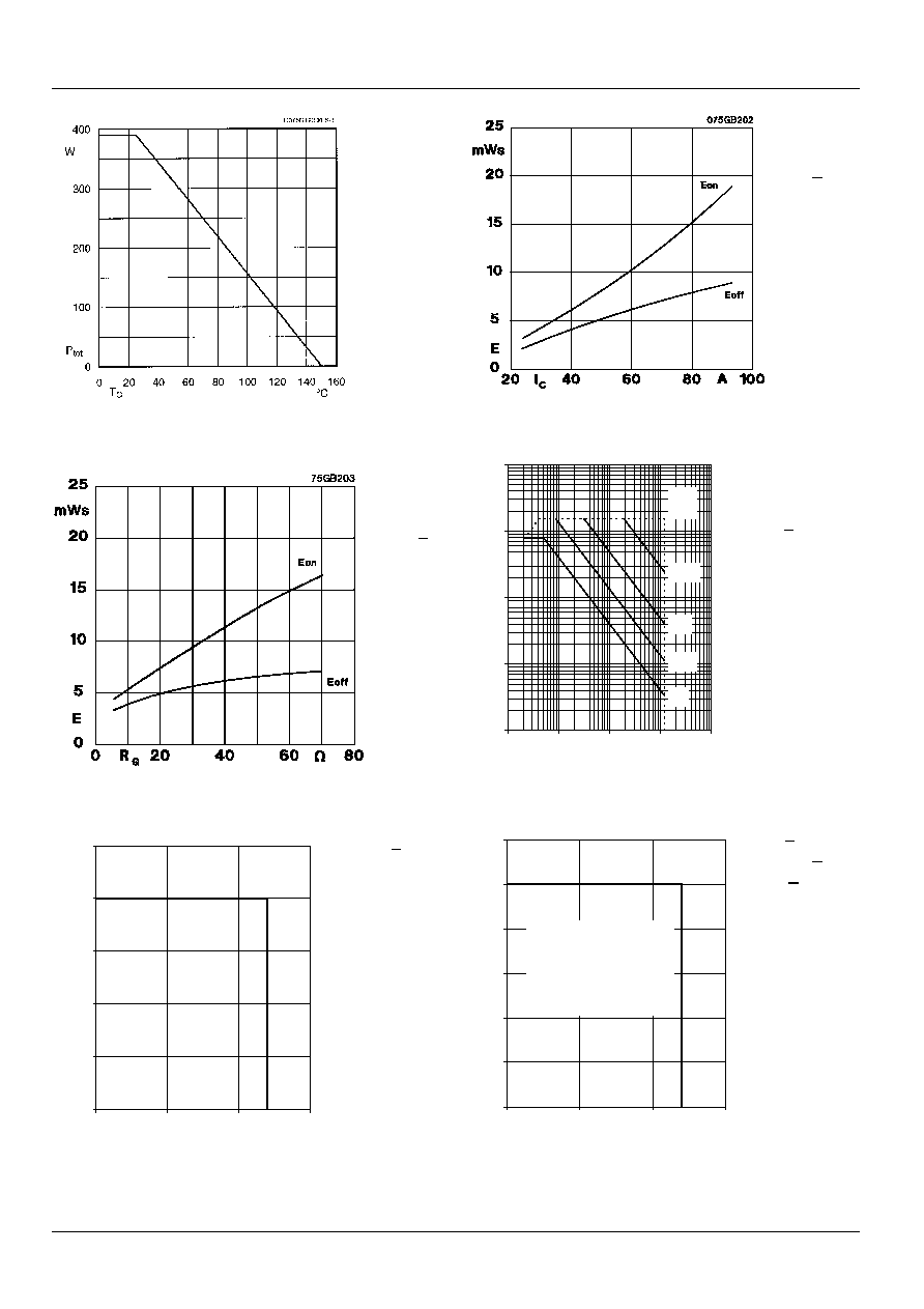
Fig. 1 Rated power dissipation P
tot
= f (T
C
)
Fig. 2 Turn-on /-off energy = f (I
C
)
Fig. 3 Turn-on /-off energy = f (R
G
)
Fig. 4 Maximum safe operating area (SOA) I
C
= f (V
CE
)
Fig. 5 Turn-off safe operating area (RBSOA)
Fig. 6 Safe operating area at short circuit I
C
= f (V
CE
)
0
P
s
PV
XV
WS�
XV
,& >$@
LXYSR
9&( >9@
0
0,5
1
1,5
2
2,5
0
500
1000
1500
ICpuls/IC
502rso.vpo
VCE [V]
0
2
4
6
8
10
12
0
500
1000
1500
Note:
*Allowed numbers of
short circuit:<1000
*Time between short
circuit:>1s
ICSC/ICN
502soas.vpo
VCE [V]

© by SEMIKRON
B 6 ≠ 227
0898
T
j
= 150 ∞C
V
GE
> 15 V
P
cond(t)
= V
CEsat(t)
. I
C(t)
V
CEsat(t)
= V
CE(TO)(Tj)
+ r
CE(Tj)
. I
C(t)
V
CE(TO)(Tj)
1,5 + 0,002 (T
j
- 25) [V]
typ.: r
CE(Tj)
= 0,020 + 0,00008 (T
j
- 25) [
]
max.: r
CE(Tj)
= 0,030 + 0,00010 (T
j
- 25) [
]
valid for V
GE
= + 15
+
2
-
1
[V]; I
C
0,3 I
Cnom
Fig. 11 Saturation characteristic (IGBT)
Calculation elements and equations
Fig. 12 Typ. transfer characteristic, t
p
= 80
µ
s; V
CE
= 20 V
Fig. 8 Rated current vs. temperature I
C
= f (T
C
)
Fig. 9 Typ. output characteristic, t
p
= 80
µ
s; 25 ∞C
Fig. 10 Typ. output characteristic, t
p
= 80
µ
s; 125 ∞C
0
20
40
60
80
100
0
1
2
3
4
5
17V
13V
15V
11V
9V
7V
IC [A]
VCE [V]
502us3.vpo
0
20
40
60
80
100
0
1
2
3
4
5
9V
7V
13V
15V
17V
11V
IC [A]
502us7.vpo
VCE [V]
,& >$@
JIYSR
9*( >9@

© by SEMIKRON
B 6 ≠ 228
0898
SKD 75 GAL 123 D
V
GE
= 0 V
f = 1 MHZ
T
j
= 125 ∞C
V
CE
= 600 V
V
GE
= + 15 V
I
C
= 50 A
induct. load
I
Cpuls
= 50 A
T
j
= 125 ∞C
V
CE
= 600 V
V
GE
= + 15 V
R
Gon
= 22
R
Goff
= 22
induct. load
Fig. 15 Typ. switching times vs. I
C
Fig. 16 Typ. switching times vs. gate resistor R
G
Fig. 17 Typ. CAL diode forward characteristic
Fig. 18 Diode D8 turn-off energy dissipation per pulse
Fig. 13 Typ. gate charge characteristic
Fig. 14 Typ. capacitances vs.V
CE
0
2
4
6
8
10
12
14
16
18
20
0
100
200
300
400
600V
800V
VGE [V]
502Qg3.vpo
QG [nC]
0,1
1
10
100
0
10
20
30
40
Ciss
Coss
Crss
C [nF]
502C.vpo
VCE [V]
10
100
1000
20
40
60
80
100
120
tdoff
tf
tr
tdon
t [ns]
502tic.vpo
IC [A]
WI
WGRII
WGRQ
WU
W >QV@
WUJYSR
5* >::@
M040GD12.X LS -18
,
$
(
411
P-
100
#
*
'
&&
'
%
M
S
'
*(
[ '

© by SEMIKRON
B 6 ≠ 229
0898
© by SEMIKRON
B 6 ≠ 230
0898
SKD 75 GAL 123 D
This is an electrostatic discharge
sensitive device (ESD).
Please observe the international
standard IEC 747-1, Chapter IX.
Two devices are supplied in one
SEMIBOX A.
Larger Packing units (10 and 20
pieces) are used if suitable.
SEMIBOX
C - 1.
Characteristics
Symbol
Conditions
1)
Values
Units
min.
typ.
max.
Input
Bridge Rectifier D1...D6
V
RRM
1400
≠
≠
V
I
D
T
case
= 80 ∞C;
≠
≠
100
A
V
F
T
vj
= 25 ∞C; I
F
= 75 A
≠
≠
1,45
V
V
TO
T
vj
= 150 ∞C
≠
≠
0,8
V
r
T
T
vj
= 150 ∞C
≠
≠
8,5
m
R
thjc
D1...D6
1,0
K/W
T
solder
> 5 s max. 15 sec. (transfer)
≠
180
250
∞C
Mechanical Data
M1
to heatsink, SI Units
(M5)
4
≠
5
Nm
to heatsink, US Units
35
≠
44
lb.in.
a
≠
≠
5x9,81
m/s
2
w
≠
≠
175
g
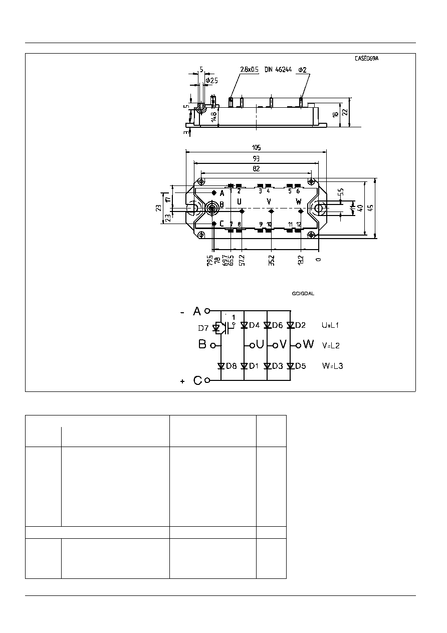
Fig. 21 Case outline and circuit diagram
SEMITRANS
Sixpack modified
Case D 69 A
UL recognition
File E63 532
*) Plastic collar around
pin B for UL creepage
distance of > 12,7 mm.
Dimensions in mm
*)