 | –≠–ª–µ–∫—Ç—Ä–æ–Ω–Ω—ã–π –∫–æ–º–ø–æ–Ω–µ–Ω—Ç: SKHI10 | –°–∫–∞—á–∞—Ç—å:  PDF PDF  ZIP ZIP |
SEMIDRIVER
TM
High Power IGBT Driver
SKHI 10/12
Features
Typical Applications
1)
2)
3)
4)
Absolute Maximum Ratings
Symbol
Conditions
Values
Units
Characteristics
Symbol
Conditions
min.
typ.
max.
Units
This technical information specifies semiconductor devices but promises no
characteristics. No warranty or guarantee expressed or implied is made regarding
delivery, performance or suitability.
SKHI 10/12
1
22-08-2003 MHW
© by SEMIKRON
© by SEMIKRON 22-08-2003
Driver Electronic ≠ PCB Drivers
1939
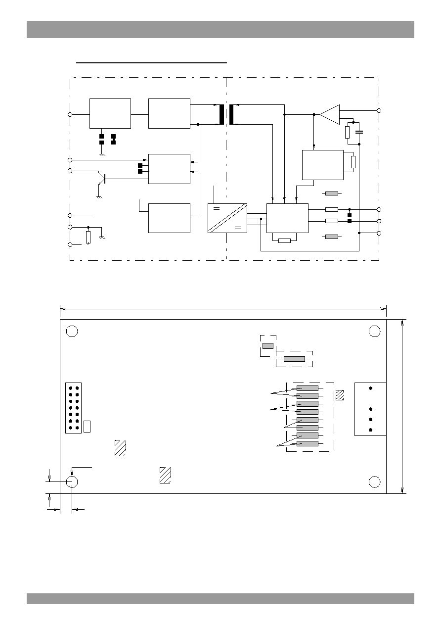
Fig.1 The numbers refer to the description on page 4, section B.
Fig.2 Dimensions (in mm) and connections of the SKHI 10
MONITOR
MEMORY
BUFFER
ERROR
INPUT
Vs
Vs
+15V
0V
10,11
1
8,9
Vs
5V
LEVEL
15V
INPUT
Vin
RESET
ERROR
2
4
3
OUTPUT
BUFFER
IRgoff
- 8V
DC/DC
CONVERTER
Vs
+15V
ISOLATION
3
Rgoff
Goff
E
2
1
MONITORING
TURN-OFF
SOFT
VCE
J2
RCE
CCE
Rgon
SC
Rgoff
VCE
Gon
5
Block diagram SKHI10
J1
primary side
secondary side
1
2
3
4
5
6
7
8
9
10
J3
SELECTOR
1
0
4.5
4.5
Rgoff-SC
Rgoff
Rgon
124
IRgoff
Input Level
1
2
4x3.5
13
14
Input
Connector
J1
66
Connector
Output
J2
1
3
2
5
CCE
RCE
ERROR logic
J3
0
Input connector = 14 pin flat cable according to DIN 41651
Output connector = MOLEX 41791 Series (mates with 41695 crimp terminal housing and crimp terminals 7258)

1940
Driver Electronic ≠ PCB Drivers
22-08-2003
© by SEMIKRON
SEMIDRIVER
TM
SKHI 10
SEMIDRIVER
TM
SKHI 10/17
High Power Single IGBT Driver
General
The intelligent single IGBT driver, SKHI10 respectively
SKHI 10/17 is a standard driver for all power IGBTs on
the market.
The high power output capability was designed to switch
high current modules or several paralleled IGBTs even for
high frequency applications. The output buffer has been
improved to make it possible to switch up to 400A IGBT
modules at frequencies up to 20kHz.
A new function has been added to the short circuit
protection circuitry (Soft Turn Off), this automatically
increases the IGBT turn off time and hence reduces the
DC voltage overvoltage spikes, enabling the use of higher
DC-bus voltages. This means an increase in the final
output power. An integrated DC/DC converter with high
galvanic isolation (4 kV) ensures that the user is
protected from the high voltage (secondary side).
The power supplies for the driver may be the same as
used in the control board (0/+15V) without the
requirement of isolation. All information that is transmitted
between input and output uses ferrite transformers,
resulting in high dv/dt immunity (75kV/
µ
s).
The driver input stage is connected directly to the control
board output and due to different control board operating
voltages the SKHI10's input circuit includes a user voltage
level selector (+15V or +5V).
In the following only the designation SKHI 10 is used.
This is valid for both driver versions. If something is to be
explained special to SKHI 10/17 it will be descriped by
marking SKHI 10/17.
A. Features and Configuration of the Driver
A short description is given below. For detailed
information, please refer to section B.
a) The SKHI10 has an INPUT LEVEL SELECTOR circuit
which is adusted by J1 for two different levels. It is
present for CMOS (15V) level, but can be changed by
the user to HCMOS (5V) level by solder bridging the
pads marked J1 together. For long input cables, we do
not recommend the 5V level due to possible
disturbances emitted by the power side.
b) The ERROR MEMORY blocks the transmission of all
turn-on signals to the IGBT if either a short circuit or
malfunction of V
S
is detected, and sends a signal to
the external control board through an open collector
transistor.
c) With a FERRITE TRANSFORMER the information
between primary and secondary may flow in both
directions and high levels of dv/dt and isolation are
obtained.
d) A high frequency DC/DC CONVERTER avoids the
requirement of external isolated power supplies to
obtain the necessary gate voltage. An isolated ferrite
transformer in half-bridge configuration supplies the
necessary power to the gate of the IGBT. With this
feature, we can use the same power supply used in
the external control circuit, even if we are using more
than one SKHI10, e.g. in H-bridge configurations.
e) Short circuit protection is provided by measuring the
collector-emitter voltage with a V
CE
MONITORING
circuit. An additional circuit detects the short circuit
after a delay (determined by R
CE
,C
CE
) and decreases
the turn off speed (adjusted by R
goff
-SC) of the IGBT.
SOFT TURN-OFF under fault conditions is necessary
as it reduces the voltage overshoot and allows for a
faster turn off during normal operation.
f) The OUTPUT BUFFER is responsible for providing the
correct current to the gate of the IGBT. If these signals
do not have sufficient power, the IGBT will not switch
properly, and additional losses or even the destruction
of the IGBT may occur. According to the application
(switching frequency and gate charge of the IGBT) the
equivalent value of R
gon
and the R
goff
must be matched
to the optimum value. This can be done by putting
additional parallel resistors R
gon
, R
goff
with those
already on the board. If only one IGBT is to be used,
(instead of parallel connection) only one cable could
be connected between driver and gate by soldering
the two J2 areas together.
Fig.1 shows a simplified block diagram of the SKHI10
driver. Some preliminary remarks will help the
understanding:
∑ Regulated +15V must be present between pins 8,9 (V
s
)
and 10,11 (
); an input signal (ON or OFF command to
the IGBTs) from the control system is supplied to pin 2
(V
in
) where HIGH=ON and LOW=OFF.
∑ Pin 5 (V
CE
) at secondary side is normally connected to
the collector of the IGBT to monitor V
CE
, but for initial
tests without connecting the IGBT it must be connected
to pin 1 (E) to avoid ERROR signal and enable the
output signals to be measured.
∑ The RESET input must be connected to 0V to enable
the V
in
signal. If it is left opened, the driver will be
blocked.
∑ To monitor the error signal, a pull-up resistor must be
provided between pin 3 (ERROR) and V
S
.
B. Description of the Circuit Block Diagram
(Fig. 1)
The circuit in Fig. 1 shows the input on the left and output
on the right (primary/secondary).
1. Input level circuit
This circuit was designed to accept two different logic
voltage levels. The standard level is +15V (factory
adjusted) intended for noisy environments or when long
connections (l > 50 cm) between the external control
circuit and SKHI10 are used, where noise immunity must
be considerate. For lower power, and short connections
between control and driver, the TTL-HCMOS level (+5V)
© by SEMIKRON 22-08-2003
Driver Electronic ≠ PCB Drivers
1941
can be selected by carefully soldering the small areas of
J1 together, specially useful for signals coming from
µ
P
based controllers.
Fig.3 Selecting J1 for 5V level (TTL)
When connecting the SKHI10 to a control board using
short connections no special attention needs to be taken
(Fig. 4a).
Fig.4a Connecting the SKHI10 with short cable
Fig.4b Conneeting the SKHI10 with long cable
Otherwise, if the length is 50cm or more (we suggest to
limit the cable length to about 1 meter), some care must
be taken. The TTL level should be avoided and CMOS/
15V is to be used instead; flat cable must have the pairs
of conductors twisted or be shielded to reduce EMI/RFI
susceptibility (Fig. 4b). If a shielded cable is used, it can
be connected to pin 1. It is coupled to 0V through a
resistor (0
).
As the input impedance of the INPUT LEVEL
SELECTOR circuit is very high, an internal pull-down
resistor keeps the IGBT in OFF state in case the Vin
connection is interrupted or left non connected.
2. Input buffer
This circuit enables and amplifies the input signal V
in
to
be transferred to the pulse transformer when RESET
(pin 4) is LOW and also prevents spurious signals being
transmitted to the secondary side.
The following overview is showing the input treshold
voltages
V
IT+
(High)
min
typ
max
15 V
9,5 V
11,0 V
12,5 V
5 V
1,8 V
2,0 V
2,4 V
3. Error memory and reset signal
The ERROR memory is triggered only by following
events:
∑ short circuit of IGBTs
∑ V
S-
undervoltage
In case of short circuit, the V
CE
monitor sends a trigger
signal (fault signal) through the impulse transformer to a
FLIP-FLOP on the primary side giving the information to
an open-collector transistor (pin 3), which may be
connected to the external control circuit as ERROR
message in HIGH logic (or LOW if J3 is short-circuited). If
V
S
power supply falls below 13V for more than 0,5ms, the
same FLIP-FLOP is set and pin 3 is activated. For HIGH
logic (default), an external R
C
must be connected
preferentiatty in the control main board. In this way the
connection between main board and driver is also
checked.
If low-logic version is used (J3 short-circuited), an internal
pull-up resistor (internally connected to V
S
) is provided,
and the signal from more SKHI10s can be connected
together to perform an wired-or-circuit.
Fig.5 Driver status information ERROR, and RESET
The ERROR signal may be disabled either by
RESET=HIGH (pin4) or by switching the power supply
(V
S
) off. The width of the RESET pulse must be more
than 5
µ
s, and in case of interrupted connection an
internal pull-up resistor will act.
1
) default logic (HIGH); for LOW logic the signals are
complementary
Table 1 ERROR signal truth table
The open-collector transistor (pin 3) may be connected
through a pull-up resistor to an extemal (intemal V
S
for the
``low-logixc`` version) vorltage supply +5V...+24V, limiting
the current to l
sink
6mA.
V
IT-
(Low)
min
typ
max
15 V
3,6 V
4,2 V
4,8 V
5 V
0,50 V
0,65 V
0,80 V
FAULT
RESET
ERROR
1)
V
in
no
0
0
enable
no
1
0
disable
yes
0
1
disable
yes
1
0
disable
1942
Driver Electronic ≠ PCB Drivers
22-08-2003
© by SEMIKRON
4. Power supply (Vs) monitor
The supply voltage V
S
is monitored. If it falls below 13V
an ERROR signal is generated and the turn-on pulses for
the IGB's gate are blocked.
5. Pulse transformer
It transmits the turn-on and turn-off signals to the IGBT. In
the reverse direction the ERROR signal from the V
CE
monitoring is transmitted via the same transformer. The
isolation is 4 kV.
6. DC/DC converter
In the primary side of the converter, a half-bridge inverter
transfers the necessary energy from V
S
to the secondary
of a ferrite transformer. In the secondary side, a full bridge
and filters convert the high frequency signal coming from
the primary to DC levels (+15V/- 8V) that are stabilised by
a voltage regulator circuit.
7. Output buffer
The output buffer is supplied by the +15V/- 8V from the
DC/DC converter. If the operation proceeds normally (no
fault), the on- and off-signal is transmitted to the gate of
an IGBT through R
gon
and R
goff
. The output stage has a
MOSFET pair that is able to source/sink up to 8A peak
current to/from the gate improving the turn-on/off time of
the IGBT. Additionally, we can select I
Rgoff
(see Fig. 2)
either to discharge the gate capacitance with a voltage
source (standard) or with a current source, specially
design for the 1700V IGBT series (it speeds up the
turn-off time of the IGBT). The present factory setting is
voltage source (I
Rgoff
= 0
). Using the current source
I
Rgoff
, R
goff
must be 0
.
Fig.6 V
CEref
waveform with parameters R
CE
, C
CE
8. Soft turn-off
In case of short-circuit, a further circuit (SOFT
TURN-OFF) increases the resistance in series with R
goff
and turns-off the IGBT at a lower speed. This produces a
smaller voltage spike (due LSTRAY x di/dt) above the DC
link by reducing the di/dt value. Because in short-circuit
conditions the Homogeneous IGBT's peak current
increases up to 8 times the nominal current (up to 10
times with Epitaxial IGBT structures), and some stray
inductance is ever present in power circuits, it must fall to
zero in a longer time than at normal operation. This "soft
3
2
1
1µ
3µ
5µ
7µ
9µ sec
18
14
10
6
2
Volt
RCE=100K
CCE=1nF
RCE=18K
CCE=330pF
RCE=10K
CCE=10pF
V
CEstat1
V
CE
V
CEsat
IGBT
turn-on
V
CEref
= f(RCE,CCE)
t
min1
t
min2
V
CEstat2
turn-off time" can be reduced by connecting a parallel
resistor R
goff
-SC (see Fig. 2) with those already on the
printed circuit board.
9. V
CE
monitoring
This circuit is responsible for short-circuit sensing. Due to
the direct measurement of V
CEstat
on the IGBT's collector,
it blocks the output buffer (through the soft turn-off circuit)
in case of short-circuit and sends a signal to the ERROR
memory on the primary side. The recognition of which
V
CE
level must be considered as a short circuit event, is
adjusted by R
CE
and C
CE
(see Fig. 2), and it depends of
the IGBT used. Typical values R
CE
=18k
and C
CE
=330
pF for SKHI 10 are delivered from factory (Fig. 6, curve
2). Using SKHI 10/17 the driver will be delivered with R
CE
= 36 k
and C
CE
= 470 pF from factory.
The V
CEref
is not static but a dynamic reference which has
an exponential shape starting at about 15V and
decreases to V
CEstat
(5V
V
CEstat
10V determinated by
R
CE
), with a time constant
(0,5
µ
s
1ms controlled
by C
CE
). The V
CEstat
must be adjusted to remain above
V
CEsat
in normal operation (the IGBT is already in full
saturation).
To avoid a false failure indication when the IGBT just
starts to conduct (V
CEsat
value is still too high) some
decay time must be provided for the V
CEref
. As the V
CE
signal is internally limited at 10V, the decay time of V
CEref
must reach this level after V
CE
or a failure indication will
occur (see Fig.6, curve 1). A t
min
is defined as function of
V
CEstat
and
to find out the best choice for R
CE
and V
CE
(see Fig.6, curve 2). The time the IGBT come to the 10V
(represented by a ,, " in Fig. 6) depends on the IGBT
itself and R
gon
used.
The R
CE
and C
CE
values can be found from Fig. 7 by
taking the V
CEstat
and t
min
as input values with following
remarks:
∑ R
CE
> 10K
∑ C
CE
< 2,7nF
Attention!: If this function is not used, for example during
the experimental phase, the V
CE
MONITORING must be
connected with the EMITTER output to avoid possible
fault indication and consequent gate signal blokking.
10. R
gon
, R
goff
These two resistors are responsible for the switching
speed of each IGBT. As an IGBT has input capacitance
(varying during the switching time) which must be
charged and discharged, both resistors will dictate what
time must be taken to do this. The final value of
resistance is difficult to predict, because it depends on
many parameters, as follows:
∑ DC-link voltage
∑ stray inductance of the circuit
∑ switching frequency
∑ type of IGBT