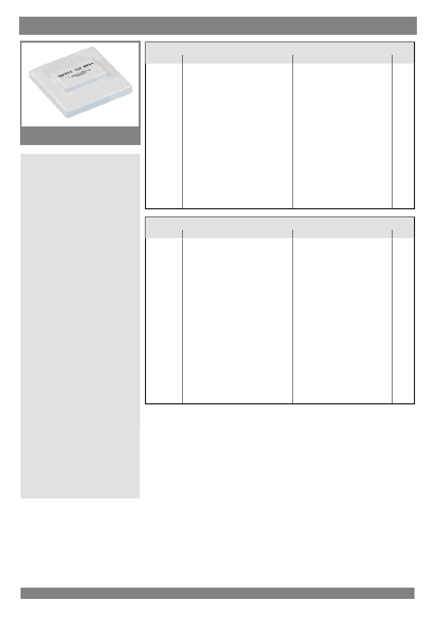
 | –≠–ª–µ–∫—Ç—Ä–æ–Ω–Ω—ã–π –∫–æ–º–ø–æ–Ω–µ–Ω—Ç: SKHI22A | –°–∫–∞—á–∞—Ç—å:  PDF PDF  ZIP ZIP |
SEMIDRIVER
TM
Hybrid Dual MOSFET
Driver
SKHI 21A
Preliminary Data
Features
Typical Applications
1)
2)
Absolute Maximum Ratings
Symbol
Conditions
Values
Units
Characteristics
Symbol
Conditions
min.
typ.
max.
Units
This technical information specifies semiconductor devices but promises no
characteristics. No warranty or guarantee expressed or implied is made regarding
delivery, performance or suitability.
SKHI 21A ...
1
18-03-2005 MHW
© by SEMIKRON

SEMIDRIVER
TM
Hybrid Dual IGBT Driver
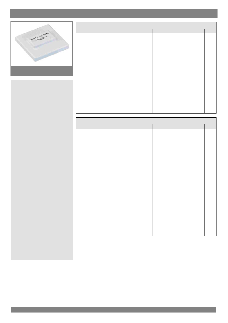
SKHI 22 A / B
Preliminary Data
Features
Typical Applications
1)
2)
Absolute Maximum Ratings
Symbol
Conditions
Values
Units
Characteristics
Symbol
Conditions
min.
typ.
max.
Units
This technical information specifies semiconductor devices but promises no
characteristics. No warranty or guarantee expressed or implied is made regarding
delivery, performance or suitability.
SKHI 22 A / B
1
18-03-2005 MHW
© by SEMIKRON
SEMIDRIVER
TM
Hybrid Dual IGBT Driver
SKHI 22 A/B H4
Preliminary Data
Features
Typical Applications
1)
2)
Absolute Maximum Ratings
Symbol
Conditions
Values
Units
Characteristics
Symbol
Conditions
min.
typ.
max.
Units
This technical information specifies semiconductor devices but promises no
characteristics. No warranty or guarantee expressed or implied is made regarding
delivery, performance or suitability.
SKHI 22 A/B H4 ...
1
18-03-2005 MHW
© by SEMIKRON
© by SEMIKRON 12-08-2004
Driver Electronic ≠ PCB Drivers
1905
External Components
4)
Higher resistance reduces free-wheeling diode peak recovery current, increases IGBT turn-on time.
5)
Higher resistance reduces turn-off peak voltage, increases turn-off time and turn-off power dissipation
Component
Function
Recommended Value
R
CE
Reference voltage for V
CE
-monitoring
with R
VCE
= 1k
(1700V IGBT):
10k
< R
CE
< 100k
18k
for SKM XX 123 (1200V)
36k
for SKM XX 173 (1700V)
C
CE
Inhibit time for V
CE
- monitoring
C
CE
< 2,7nF
0,33nF for SKM XX 123 (1200V)
0,47nF for SKM XX 173 (1700V)
0,5µs < t
min
< 10µs
R
VCE
Collector series resistance for 1700V
IGBT-operation
1k
/ 0,4W
R
ERROR
Pull-up resistance at error output
1k
< R
ERROR
< 10k
R
GON
Turn-on speed of the IGBT
4)
R
GON
> 3
R
GOFF
Turn-off speed of the IGBT
5)
R
GOFF
> 3
V
CEstat
V
( )
10 R
CE
k
(
)
10
R
CE
k
(
)
+
------------------------------------
1,4 (1)
≠
=
V
CEstat
V
( )
10 R
CE
k
(
)
10
R
CE
k
(
)
+
------------------------------------
1,8 (1.1)
≠
=
t
min
CE
15
V
CEstat
V
( )
≠
10
V
CEstat
V
( )
≠
---------------------------------------- (2)
ln
=
CE
µ
s
( )
C
CE
nF
( )
10 R
CE
k
(
)
10
R
CE
k
(
)
+
------------------------------------ (3)
=
U
Pull
Up
≠
R
ERROR
-----------------------
15mA
<
1906
Driver Electronic ≠ PCB Drivers
12-08-2004
© by SEMIKRON
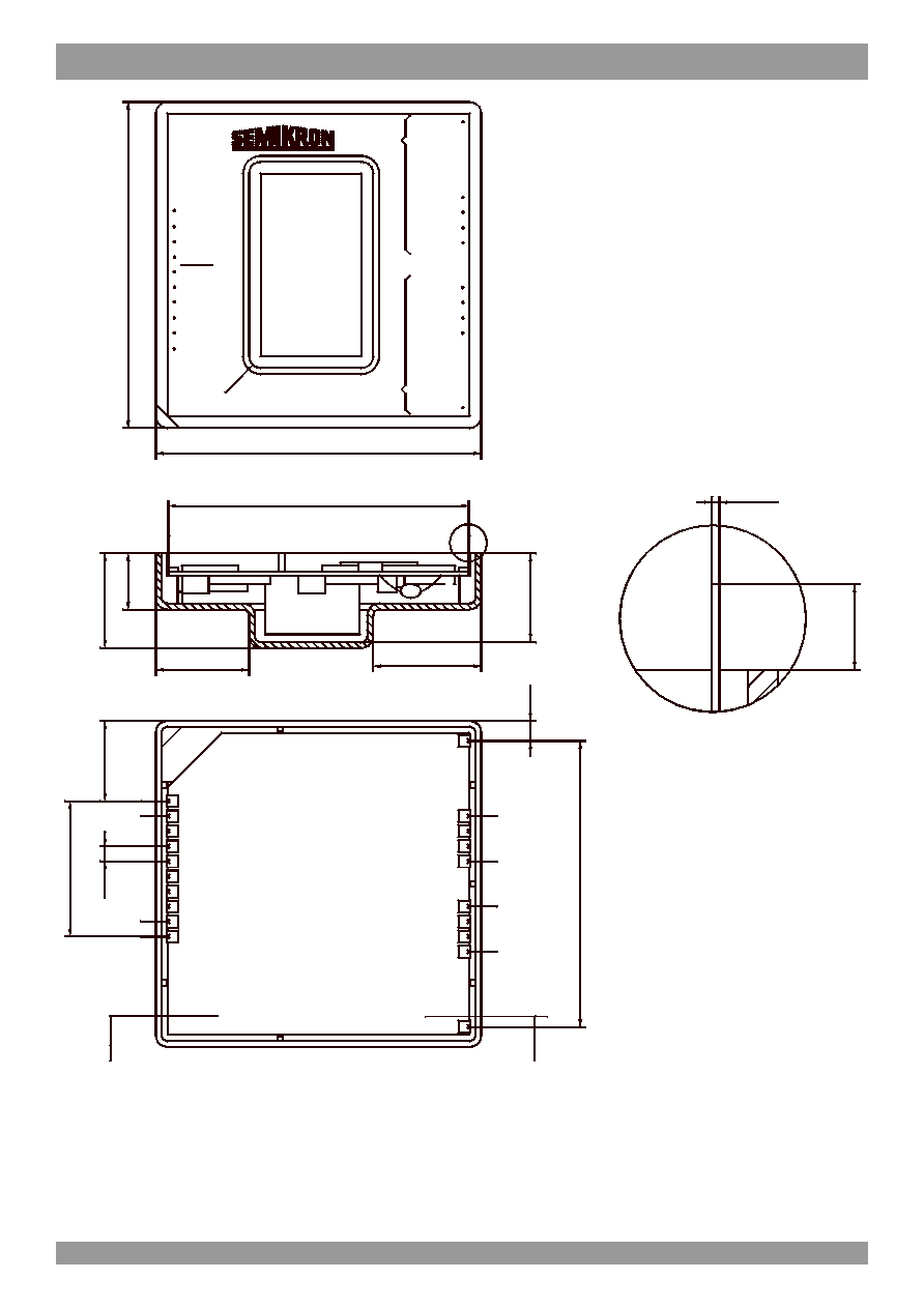
PIN array
Fig. 2 shows the pin arrays. The input side (primary side) comprises 10 inputs (SKHI 22A / 21A 8 inputs), forming the
interface to the control circuit (see fig.1).
The output side (secondary side) of the hybrid driver shows two symmetrical groups of pins with 4 outputs, each forming
the interface to the power module. All pins are designed for a grid of 2,54 mm.
Primary side PIN array
ATTENTION: Inputs P6 and P5 are not existing for SKHI 22A/ 21A. The contactor tracks of the digital input signals P5/
P6/ P9 must not be longer than 20 mm to avoid interferences, if no bridges are connected.
Secondary side PIN array
ATTENTION: The connector leads to the power module should be as short as possible.
PIN No. Designation
Explanation
P14
GND / 0V
related earth connection for input signals
P13
V
S
+ 15V
±
4% voltage supply
P12
V
IN1
switching signal input 1 (TOP switch)
positive 5V logic (for SKHI22A /21A, 15V logic)
P11
free
not wired
P10
/ERROR
error output, low = error; open collector output; max 30V / 15mA
(for SKHI22A /21A, internal 10k
pull-up resistor versus V
S
)
P9
TDT2
signal input for digital adjustment of interlocking time;
SKHI22B: to be switched by bridge to GND (see fig. 3)
SKHI22A /21A: to be switched by bridge to V
S
P8
V
IN2
switching signal input 2 (BOTTOM switch);
positive 5V logic (for SKHI22A /21A, 15V logic)
P7
GND / 0V
related earth connection for input signals
P6
SELECT
signal input for neutralizing locking function;
to be switched by bridge to GND
P5
TDT1
signal input for digital adjustment of locking time;
to be switched by bridge to GND
PIN No. Designation Explanation
S20
V
CE1
collector output IGBT 1 (TOP switch)
S15
C
CE1
reference voltage adjustment with R
CE
and C
CE
S14
G
ON1
gate 1 R
ON
output
S13
G
OFF1
gate 1 R
OFF
output
S12
E1
emitter output IGBT 1 (TOP switch)
S1
V
CE2
collector output IGBT 2 (BOTTOM switch)
S6
C
CE2
reference voltage adjustment with R
CE
and C
CE
S7
G
ON2
gate 2 R
ON
output
S8
G
OFF2
gate 2 R
OFF
output
S9
E2
emitter output IGBT 2 (BOTTOM switch)
© by SEMIKRON 12-08-2004
Driver Electronic ≠ PCB Drivers
1907
I
G
B
T
-
M
o
d
u
l
e
S
E
M
I
T
R
A
N
S
o
u
t
p
u
t
2
(
B
O
T
T
O
M
)
L
O
A
D
o
u
t
p
u
t
1
(
T
O
P
)
=
I
s
o
l
a
t
i
o
n
-
i
n
p
u
t
b
u
f
f
e
r
-
s
h
o
r
t
p
u
l
s
e
s
u
p
r
e
s
s
i
o
n
-
p
u
l
s
e
s
h
a
p
e
r
V
C
E
R
S
2
0
c
u
r
r
e
n
t
V
C
E
*
o
v
e
r
*
*
S
1
2
S
1
3
S
1
4
S
1
5
c
u
r
r
e
n
t
P
o
w
e
r
d
r
i
v
e
r
o
v
e
r
R
4
C
E
R
3
C
E
C
C
E
V
S
1
R
o
f
f
*
*
o
n
V
C
E
R
1
5
=
d
r
i
v
e
r
P
o
w
e
r
s
e
c
o
n
d
a
r
y
s
i
d
e
7
C
E
S
7
S
8
S
6
o
n
R
o
f
f
R
R
6
C
C
E
*
S
9
o
u
t
p
u
t
2
i
n
p
u
t
1
(
T
O
P
)
6
k
8
/
1
0
0
V
P
1
2
i
T
3
k
2
T
D
T
1
S
E
L
E
C
T
E
r
r
o
r
T
D
T
2
G
N
D
/
O
V
G
N
D
/
O
V
(
B
O
T
T
O
M
)
i
n
p
u
t
i
n
p
u
t
2
*
*
*
V
*
*
*
E
R
R
O
R
R
V
*
*
*
S
=
-
i
n
t
e
r
l
o
c
k
-
d
e
a
d
t
i
m
e
6
k
8
/
1
0
0
V
P
8
i
B
P
7
3
k
2
P
5
P
1
4
P
9
P
6
V
=
S
V
S
p
r
i
m
a
r
y
s
i
d
e
i
n
t
e
g
r
a
t
e
d
i
n
A
S
I
C
-
V
s
m
o
n
i
t
o
r
-
E
r
r
o
r
m
o
n
i
t
o
r
-
E
r
r
o
r
m
e
m
o
r
y
S
V
S
P
1
3
P
1
0
V
*
W
h
e
n
S
K
H
I
2
2
B
i
s
d
r
i
v
i
n
g
1
7
0
0
V
I
G
B
T
s
,
a
1
k
/
0
,
4
W
R
VC
E
-
r
e
s
i
s
t
o
r
m
u
s
t
b
e
c
o
n
n
e
c
t
e
d
i
n
s
e
r
i
e
s
t
o
t
h
e
V
C
E
i
n
p
u
t
.
*
*
T
h
e
V
C
E
-
t
e
r
m
i
n
a
l
i
s
t
o
b
e
c
o
n
n
e
c
t
e
d
t
o
t
h
e
I
G
B
T
c
o
l
l
e
c
t
o
r
C
.
I
f
t
h
e
V
C
E
-
m
o
n
i
t
o
r
i
n
g
i
s
n
o
t
u
s
e
d
,
c
o
n
n
e
c
t
S
1
t
o
S
9
o
r
S
2
0
t
o
S
1
2
r
e
s
p
e
c
t
i
v
e
l
y
.
*
*
*
T
e
r
m
i
n
a
l
s
P
5
a
n
d
P
6
a
r
e
n
o
t
e
x
i
s
t
i
n
g
f
o
r
S
K
H
I
2
2
A
/
2
1
A
;
i
n
t
e
r
n
a
l
p
u
l
l
-
u
p
r
e
s
i
s
t
o
r
e
x
i
s
t
s
i
n
S
K
H
I
2
2
A
/
2
1
A
o
n
l
y
.
1
-
7
C
o
n
n
e
c
t
i
o
n
s
t
o
S
E
M
I
T
R
A
N
S
G
B
-
m
o
d
u
l
e
1908
Driver Electronic ≠ PCB Drivers
12-08-2004
© by SEMIKRON
Fig. 2 Dimension drawing and PIN array (P5 and P6 are not existing for SKHI22A/21A)
VCE
VCE
GOFF
GON
CCE
CCE
GON
GOFF
18.25
E
E
1
3
.
5
3
P14
A
P13
2
2
.
8
6
2
.
5
4
P6
P5
±
0
.
3
1
6
9
.
5
±
0
.
2
5
5
50.8
measured from pin-centre to pin-centre
15.75
R2
TDT1
±0.3
OUT2
±0.2
55
S
K
H
I
X
X
Y
SELECT
TDT2
V
GND/0V
V
VS
GND/0V
IN1
IN2
ERROR
OUT1
D
a
t
e
-
C
o
d
e
S15
S20
A
S12
S9
S6
4
8
.
2
6
detail "A" on scale 10 : 1
3
.
3
7
±
0
.
3
S1
1
5
A
3
.
5
±
0
.
5
0.25x0.5
© by SEMIKRON 12-08-2004
Driver Electronic ≠ PCB Drivers
1909
SEMIDRIVER
TM
SKHI 22A / 22B und SKHI 21A
Hybrid dual drivers
The driver generation SKHI 22A/B and SKHI 21A will
replace the hybrid drivers SKHI 21/22 and is suitable for all
available low and medium power range IGBT and
MOSFETs.
The SKHI 22A (SKHI 21A) is a form-, fit- and mostly
function-compatible replacement to its predecessor, the
SKHI 22 (SKHI 21).
The SKHI 22B is recommended for any new development.
It has two additional signal pins on the primary side with
which further functions may be utilized.
The SKHI 22A and SKHI 22B are available with standard
isolation (isolation testing voltage 2500 VAC, 2sec.) as
well as with an increased isolation voltage (type "H4")
(isolation testing voltage 4000 VAC, 2sec.). The SKHI 21A
is only offered with standard isolation features.
Differences SKHI 22-22A (SKHI 21-21A)
Compared to the old SKHI 22/21 the new driver
SKHI
22A / 21A is absolutely compatible with regards to
pins and mostly with regards to functions. It may be
equivalently used in existing PCBs.
The following points have to be considered when
exchanging the drivers:
∑ Leave out the two resistors RTD for interlocking
dead time adjustment at pin 11 and pin 9.
∑ The interlocking time of the driver stages in
halfbridge applications is adjusted to 3,25 µs. It may
be increased up to 4,25 µs by applying a 15 V (VS)
supply voltage at Pin 9 (TDT2) (wire bridge)
∑ The error reset time is typically 9µs.
∑ The input resistance is 10 k
.
As far as the SKHI 22A is concerned, the negative gate
voltage required for turn-off of the IGBT is no longer -15V,
but -7V.
General description
The new driver generation SKHI 22A/B, SKHI 21A
consists of a hybrid component which may directly be
mounted to the PCB.
All devices necessary for driving, voltage supply, error
monitoring and potential separation are integrated in the
driver. In order to adapt the driver to the used power
module, only very few additional wiring may be necessary.
The forward voltage of the IGBT is detected by an
integrated short-circuit protection, which will turn off the
module when a certain threshold is exceeded.
In case of short-circuit or too low supply voltage the
integrated error memory is set and an error signal is
generated.
The driver is connected to a controlled + 15 V-supply
voltage. The input signal level is 0/15 V for the SKHI 22A/
21A and 0/5 V for the SKHI 22B.
In the following explanations the whole driver family will be
designated as SKHI 22B. If a special type is referred to,
the concerned driver version will explicitly be named.
Technical explanations
1
Description of the circuit block diagram and the
functions of the driver
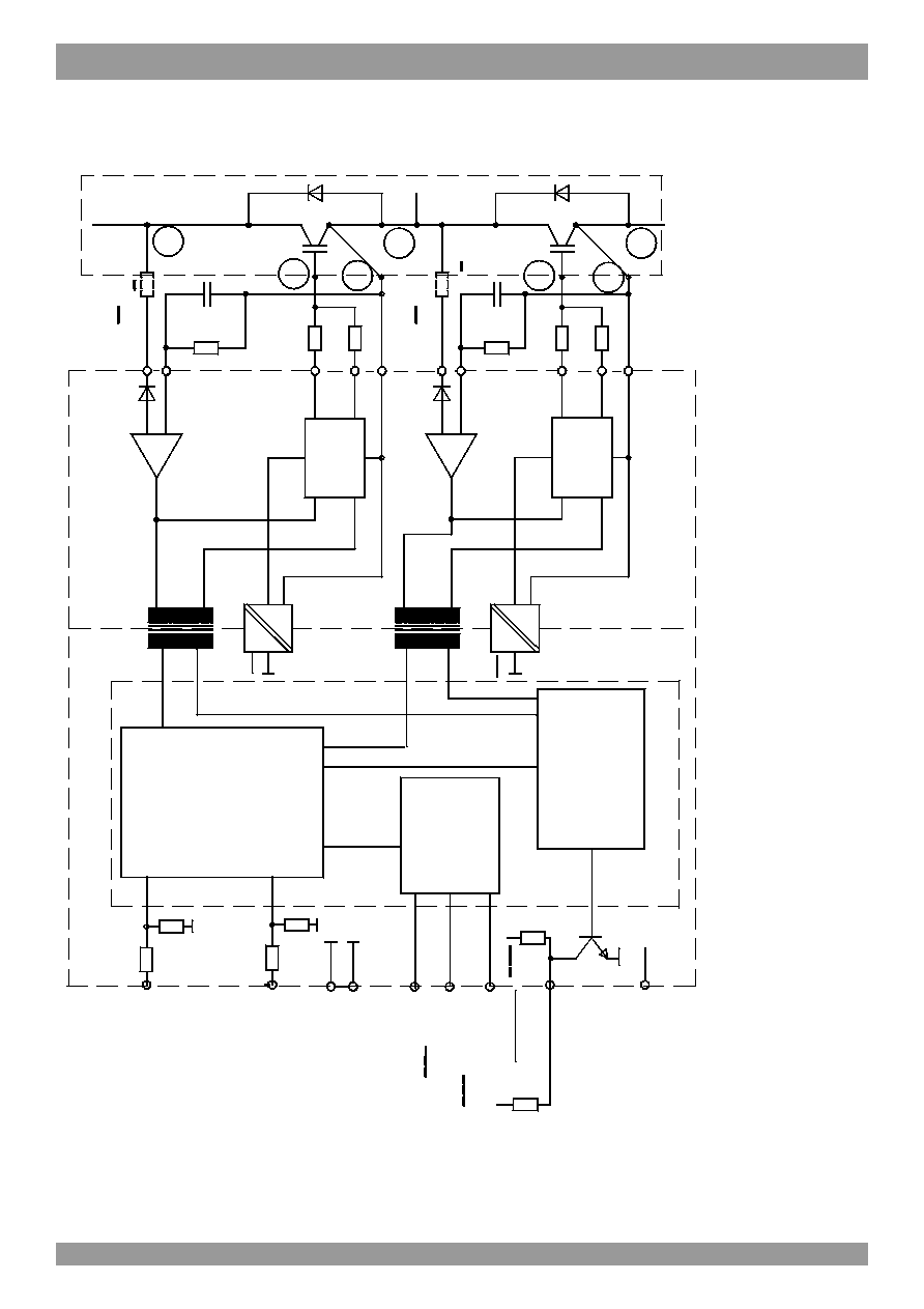
The block diagram (fig.1) shows the inputs of the driver
(primary side) on the left side and the outputs (secondary
side) on the right.
The following functions are allocated to the primary
side:
Input-Schmitt-trigger, CMOS compatible, positive logic
(input high = IGBT on)
Interlock circuit and deadtime generation of the IGBT
If one IGBT is turned on, the other IGBT of a halfbridge
cannot be switched. Additionally, a digitally adjustable
interlocking time is generated by the driver (see fig. 3),
which has to be longer than the turn-off delay time of the
IGBT. This is to avoid that one IGBT is turned on before
the other one is not completely discharged. This
protec-tion-function may be neutralized by switching the
select input (pin6) (see fig. 3). fig. 3 documents possible
interlock-times. "High" value can be achieved with no
connection and connection to 5 V as well.
Fig. 3 SKHI 22B - Selection of interlock-times:
,,High"-level can be achieved by no connection or
connecting to 5 V
Short pulse suppression
The integrated short pulse suppression avoids very short
switching pulses at the power semiconductor caused by
high-frequency interference pulses at the driver input
signals. Switching pulses shorter than 500 ns are
suppressed and not transmitted to the IGBT.
Power supply monitoring (V
S
)
A controlled 15 V-supply voltage is applied to the driver. If
it falls below 13 V, an error is monitored and the error
output signal switches to low level.
1.The following descriptions apply to the use of the hybrid
driver for IGBTs as well as for power MOSFETs. For the
reason of shortness, only IGBTs will be mentioned in the
following. The designations "collector" and "emitter" will refer
to IGBTs, whereas for the MOSFETs "drain" and "source" are
to be read instead.
P6 ;
SELECT
P5 ;
TDT1
P9 ;
TDT2
interlock time
t
TD
/µs
open / 5V
GND
GND
1,3
open / 5V
GND
open / 5V
2,3
open / 5V
open / 5V
GND
3,3
open / 5V
open / 5V
open / 5V
4,3
GND
X
X
no interlock
1910
Driver Electronic ≠ PCB Drivers
12-08-2004
© by SEMIKRON
Error monitoring and error memory
The error memory is set in case of under-voltage or
short-circuit of the IGBTs. In case of short-circuit, an error
signal is transmitted by the V
CE
-input via the pulse
transformers to the error memory. The error memory will
lock all switching pulses to the IGBTs and trigger the error
output (P10) of the driver. The error output consists of an
open collector transistor, which directs the signal to earth
in case of error. SEMIKRON recommends the user to
provide for a pull-up resistor directly connected to the error
evaluation board and to adapt the error level to the desired
signal voltage this way. The open collector transistor may
be connected to max. 30 V / 15 mA. If several SKHI 22Bs
are used in one device, the error terminals may also be
paralleled.
ATTENTION: Only the SKHI 22A / 21A is equipped with
an internal pull-up resistor of 10 k
versus V
S
. The
SKHI
22B does not contain an internal pull-up resistor.
The error memory may only be reset, if no error is pending
and both cycle signal inputs are set to low for > 9 µs at the
same time.
Pulse transformer set
The transformer set consists of two pulse transformers
one is used bidirectional for turn-on and turn-off signals of
the IGBT and the error feedback between primary and
secondary side, the other one for the DC/DC-converter.
The DC/DC-converter serves as potential-separation and
power supply for the two secondary sides of the driver.
The isolation voltage for the "H4"-type is 4000 V
AC
and
2500 V
AC
for all other types.
The secondary side consists of two symmetrical
driver switches integrating the following components:
Supply voltage
The voltage supply consists of a rectifier, a capacitor, a
voltage controller for - 7 V and + 15 V and a + 10 V
reference voltage.
Gate driver
The output transistors of the power drivers are MOSFETs.
The sources of the MOSFETs are separately connected to
external terminals in order to provide setting of the turn-on
and turn-off speed by the external resistors R
ON
and R
OFF
.
Do not connect the terminals S7 with S8 and S13 with
S14, respectively. The IGBT is turned on by the driver at +
15 V by R
ON
and turned off at - 7 V by R
OFF
. R
ON
and R
OFF
may not chosen below 3
. In order to ensure locking of
the IGBT even when the driver supply voltage is turned off,
a 22 k
-resistor versus the emitter output (E) has been
integrated at output G
OFF
.
V
CE
-monitoring
The V
CE
-monitoring controls the collector-emitter voltage
V
CE
of the IGBT during its on-state. V
CE
is internally limited
to 10 V. If the reference voltage V
CEref
is exceeded, the
IGBT will be switched off and an error is indicated. The
reference voltage V
CEref
may dynamically be adapted to
the IGBTs switching behaviour. Immediately after turn-on
of the IGBT, a higher value is effective than in the steady
state. This value will, however, be reset, when the
IGBT is turned off. V
CEstat
is the steady-state value of V
CEref
and is adjusted to the required maximum value for each
IGBT by an external resistor R
CE
to be connected between
the terminals C
CE
(S6/S15) and E (S9/S12). It may not
exceed 10 V. The time constant for the delay of V
CEref
may
be increased by an external capacitor C
CE
, which is
connected in parallel to R
CE
. It controls the time tmin which
passes after turn-on of the IGBT before the
V
CE
-monitoring is activated. This makes possible any
adaptation to the switching behavior of any of the IGBTs.
After t
min
has passed, the V
CE
-monitoring will be triggered
as soon as V
CE
> V
CEref
and will turn off the IGBT.
External components and possible adjust-
ments of the hybrid driver
Fig. 1 shows the required external components for
adjustment and adaptation to the power module.
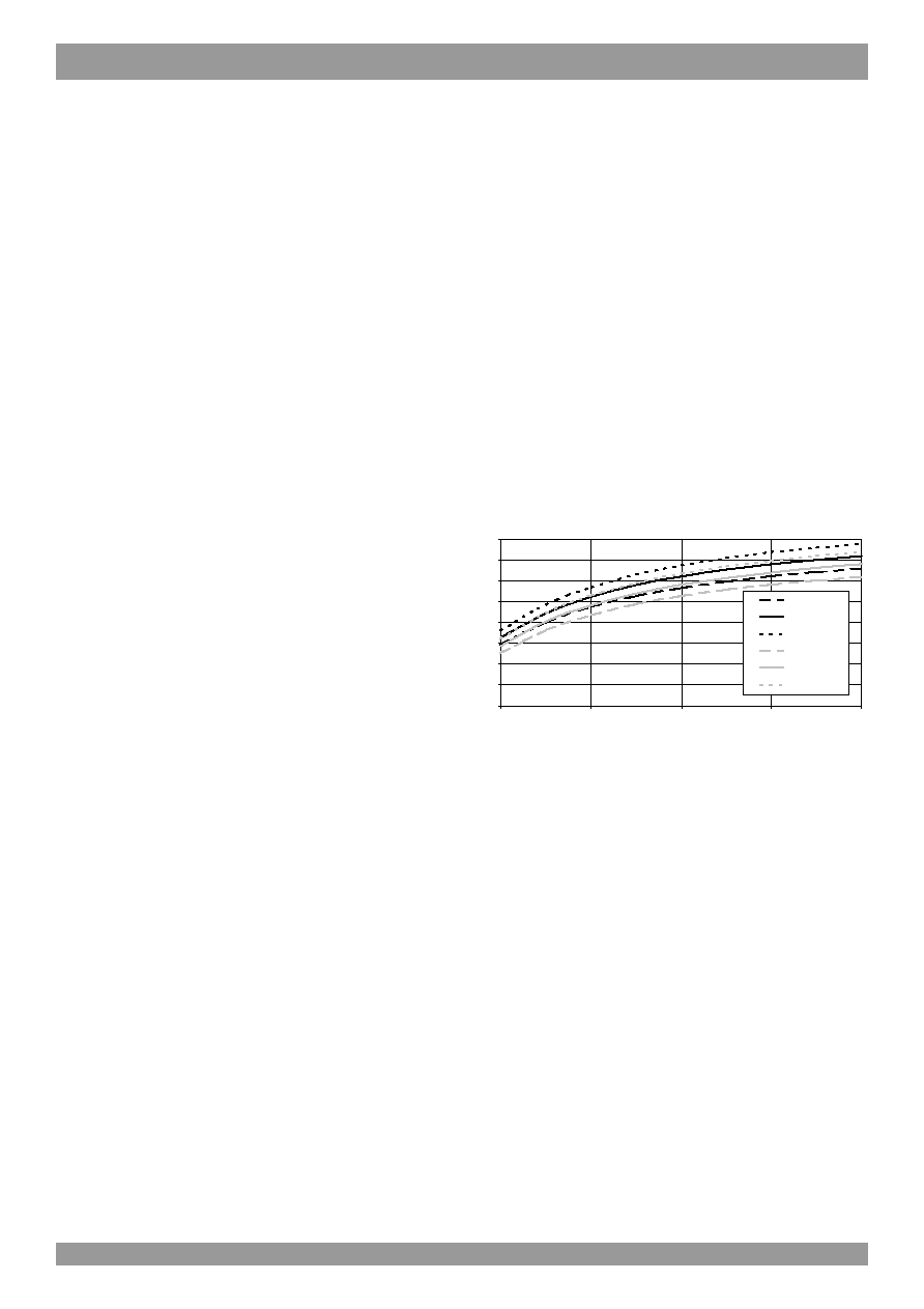
VCE - monitoring adjustment
The external components R
CE
and C
CE
are applied for
adjusting the steady-state threshold and the short-circuit
monitoring dynamic. R
CE
and C
CE
are connected in
parallel to the terminals C
CE
(S15/ S6) and E (S12/ S9) .
Fig. 4 V
CEstat
in dependence of R
CE
(T
amb
= 25∞C)
Dimensioning of R
CE
and C
CE
can be done in three steps:
1. Calculate the maximum forward voltage from the
datasheet of the used IGBT and determine V
CEstat
2. Calculate approximate value of R
CE
according to
equation (1) or (1.1) from V
CEstat
or determine R
CE
by
using fig.4.
3. Determine t
min
and calculate C
CE
according to
equations (2) and (3).
Typical values are
for 1200 V IGBT: V
CEstat
= 5 V; t
min
= 1,45 µs,
R
CE
= 18 k
, C
CE
= 330 pF
for 1700 V IGBT:
V
CEstat
= 6 V; t
min
= 3 µs,
R
CE
= 36 k
, C
CE
= 470 pF
Adaptation to 1700 V IGBT
When using 1700 V IGBTs it is necessary to connect a
1 k
/ 0,4 W adaptation resistor between the V
CE
-terminal
(S20/ S1) and the respective collector.
0
1
2
3
4
5
6
7
8
10
20
30
40
50
R
CE
/ kOhm
V
C
E
s
t
a
t
/
V
1200V (min)
1200V (typ)
1200V (max)
1700V (min)
1700V (typ)
1700V (max)
© by SEMIKRON 12-08-2004
Driver Electronic ≠ PCB Drivers
1911
Adaptation to error signal level
An open collector transistor is used as error terminal,
which, in case of error, leads the signal to earth. The signal
has to be adapted to the evaluation circuit's voltage level
by means of an externally connected pull-up resistor. The
maximum load applied to the transistor shall be 30 V / 15
mA.
As for the SKHI 22A / 21A a 10 k
pull-up resistor versus
V
S
(P13) has already been integrated in the driver.
IGBT switching speed adjustment
The IGBT switching speed may be adjusted by the
resistors R
ON
and R
OFF
. By increasing R
ON
the turn-on
speed will decrease. The reverse peak current of the
free-wheeling
diode
will
diminish.
SEMIKRON
recommends to adjust R
ON
to a level that will keep the
turn-on delay time t
d(on)
of the IGBT < 1 µs.
By increasing R
OFF
the turn-off speed of the IGBT will
decrease. The inductive peak overvoltage during turn-off
will diminish.
The minimum gate resistor value for R
OFF
and R
ON
is 3
.
Typical values for R
ON
and R
OFF
recommended by
SEMIKRON are given in fig. 5
Fig. 5 Typical values for external components
Interlocking time adjustment
Fig. 3 shows the possible interlocking times between
output1 and output2. Interlocking times are adjusted by
connecting the terminals TDT1 (P5), TDT2 (P9) and
SELECT (P6) either to earth/ GND (P7 and P14)
according to the required function or by leaving them
open.
A typical interlocking time value is 3,25 µs (P9 = GND; P5
and P6 open). For SKHI 22A / 21A the terminals TDT1
(P5) and SELECT (P6) are not existing. The interlocking
time has been fixed to 3,25 µs and may only be increased
to 4,25 µs by connecting TDT2 (P9) to V
S
(P13).
ATTENTION: If the terminals TDT1 (P5), TDT2 (P9) and
SELECT (P6) are not connected, eventually connected
track on PC-board may not be longer than 20 mm in order
to avoid interferences.
SK-IGBT-Modul
R
Gon
R
Goff
C
CE
pF
R
CE
k
R
VCE
k
SKM 50GB123D
22
22
330
18
0
SKM 75GB123D
22
22
330
18
0
SKM 100GB123D
15
15
330
18
0
SKM 145GB123D
12
12
330
18
0
SKM 150GB123D
12
12
330
18
0
SKM 200GB123D
10
10
330
18
0
SKM 300GB123D
8,2
8,2
330
18
0
SKM 400GA123D
6,8
6,8
330
18
0
SKM 75GB173D
15
15
470
36
1
SKM 100GB173D
12
12
470
36
1
SKM 150GB173D
10
10
470
36
1
SKM 200GB173D
8,2
8,2
470
36
1
SEMIKRON recommends to start-up operation using the
values recommended by SEMIKRON and to optimize the
values gradually according to the IGBT switching
behaviour and overvoltage peaks within the specific
circuitry.
Driver performance and application limits
The drivers are designed for application with halfbridges
and single modules with a maximum gate charge Q
GE
<
4
µC (see fig. 6).
The charge necessary to switch the IGBT is mainly
depending on the IGBT's chip size, the DC-link voltage
and the gate voltage.
This correlation is also shown in the corresponding
module datasheet curves.
It should, however, be considered that the SKHI 22B is
turned on at + 15 V and turned off at - 7 V. Therefore, the
gate voltage will change by 22 V during every switching
procedure.
Unfortunately, most datasheets do not indicate negative
gate voltages. In order to determine the required charge,
the upper leg of the charge curve may be prolonged to
+
22 V for determination of approximate charge per
switch.
The medium output current of the driver is determined by
the switching frequency and the gate charge. For the SKHI
22B the maximum medium output current is Iout
AVmax
< ±
40 mA.
The maximum switching frequency f
MAX
may be calculated
with the following formula, the maximum value however
being 50 kHz due to switching reasons:
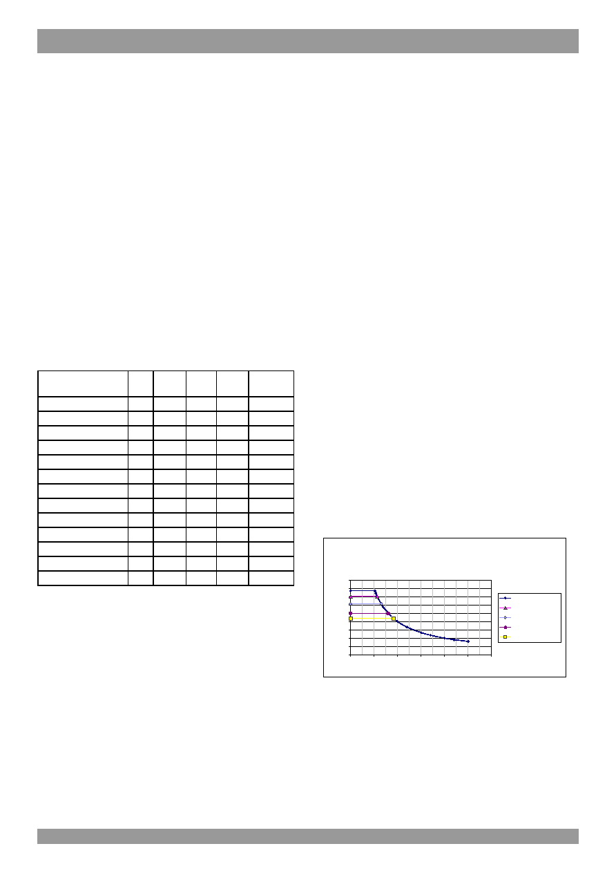
Fig. 6 shows the maximum rating for the output charge per
pulse for different gate resistors.
Fig. 6 Maximum rating for output charge per pulse
Further application notes
The CMOS-inputs of the hybrid driver are extremely
sensitive to over-voltage. Voltages higher than V
S
+
0,3
V or below ≠ 0,3 V may destroy these inputs.
Therefore, control signal over-voltages exceeding the
above values have to be avoided.
Please provide for static discharge protection during
handling. As long as the hybrid driver is not completely
assembled, the input terminals have to be short-circuited.
f
MAX
kHz
(
)
4 10
4
Q
GE
nC
(
)
-----------------------
=
SKHI 22 A/B maximum rating for output charge per
pulse
0,00
0,50
1,00
1,50
2,00
2,50
3,00
3,50
4,00
4,50
0
10
20
30
40
50
60
f / kHz
Q
/
µ
C
Rg=24 OHM; 3,86µC
Rg=18 OHM; 3,52µC
Rg=12 OHM; 3,07µC
Rg=6 OHM, 2,50µC
Rg=3 OHM, 2,18µC

1912
Driver Electronic ≠ PCB Drivers
12-08-2004
© by SEMIKRON
Persons working with CMOS-devices have to wear a
grounded bracelet. Any synthetic floor coverings must not
be statically chargeable. Even during transportation the
input terminals have to be short-circuited using, for
example, conductive rubber. Worktables have to be
grounded. The same safety requirements apply to
MOSFET- and IGBT-modules!
The connecting leads between hybrid driver and the
power module should be as short as possible, the driver
leads should be twisted.
Any parasitic inductances within the DC-link have to be
minimized. Over-voltages may be absorbed by C- or
RCD-snubbers between the main terminals for PLUS and
MINUS of the power module.
When first operating a newly developed circuit,
SEMIKRON recommends to apply low collector voltage
and load current in the beginning and to increase these
values gradually, observing the turn-off behaviour of the
free-wheeling diode and the turn-off voltage spikes
generated accross the IGBT. An oscillographic control will
be necessary. In addition to that the case temperature of
the module has to be monitored. When the circuit works
correctly under rated operation conditions, short-circuit
testing may be done, starting again with low collector
voltage.
It is important to feed any errors back to the control circuit
and to switch off the device immediately in such events.
Repeated turn-on of the IGBT into a short circuit with a
high frequency may destroy the device.
Mechanical fixing on PCB:
In applications with mechanical vibrations (vehicles)
2
do
not use a ty-rap for fixing the driver, but - after soldering
and testing - apply special glue. Recommended types:
CIBA GEIGY XP 5090 + 5091; PACTAN 5011; WACKER
A33 (ivory) or N199 (transparent), applied around the case
edge (forms a concave mould). The housing may not be
pressed on the PCB; do not twist the PCB with the driver
soldered on, otherwise the internal ceramics may crack.
The driver is not suitable for big PCBs.
SEMIKRON offers a printed circuit board (PCB) type
SKPC2006 compatible for mounting a SKHI 21A or
SKHI
22A. This PCB contains the necessary tracks to
connect the external capacitors C
CE
and resistors R
CE
,
R
on
, R
off
(see fig. 1).
The PCB may directly be plugged to SEMITRANS 3-IGBT
modules and be fixed to the heatsink by 3 thread bolts.
Dimensions: L x W x H = 96 x 67 x 1,5 mm.
For further details please contact SEMIKRON.
2.tested acceleration (x; y; z-axis):10-100 Hz: 1,5 g;
shock: 5 g (TÐV according to LES-DB-BN 411002)
This technical information specifies devices but promises no characteristics. No warranty or guarantee expressed or implied is made
regarding delivery, performance or suitability.