 | –≠–ª–µ–∫—Ç—Ä–æ–Ω–Ω—ã–π –∫–æ–º–ø–æ–Ω–µ–Ω—Ç: SKHI26F | –°–∫–∞—á–∞—Ç—å:  PDF PDF  ZIP ZIP |

SKHI 26W, SKHI 26F
© by SEMIKRON 22-08-2003
Driver Electronic ≠ PCB Drivers
1959
SEMIDRIVER
TM
Double IGBT driver
SKHI 26W, SKHI 26F
Features
∑ Double driver for half bridge
modules
∑ SKHI 26 drives all SEMIKRON
IGBT¥s with V
CE
up to 1200 V
∑ SKHI 26F has fibre optic input
∑ SKHI 26W has wire (galvanic)
input
∑ CMOS compatible inputs
∑ Short circuit protection by V
CE
monitoring and soft switch off
∑ Driver interlock top/bottom
∑ Isolation by transformers
∑ Supply undervoltage
protection (< 13 V)
∑ Error latch / open-collector
output (SKHI 26W)
∑ DC bus voltage up to 1200 V
Typical Applications
∑ High power switches or
paralleled IGBTs
∑ Driver for IGBT modules in
bridge circuits in choppers,
inverter drives, UPS
and welding inverters
Absolute Maximum Ratings
Symbol
Conditions
Values
Units
V
S
Supply voltage primary
18
V
V
iH
Input signal voltage (HIGH)
V
S
± 0,3
V
I
iH
Input signal current (HIGH)
0,34
mA
Q
Gate max
Max. output charge per pulse
± 10
µ
C
Iout
PEAK
Output peak current
± 8
A
Iout
AV
Output average current
± 100
mA
V
CE
Collector-emitter maximum voltage sense
1600
V
dv/dt
Rate of rise and fall of voltage
75
kV/
µ
s
(secondary to primary side)
V
isol lO
Isolation test volt. IN-OUT (2 sec. AC)
4000
V
T
op
Operationg temperature (SKHI 26W)
- 25 ... + 85
∞C
Operating temperature (SKHI 26F)
0 ... + 70
∞C
T
stq
Storage temperature (SKHI 26W)
- 25 ... + 85
∞C
Storage temperature (SKHI 26F)
0 ... + 70
∞C
Characteristics
T
a
= 25 ∞C, unless otherwise specified
Symbol
Conditions
min.
typ.
max. Units
V
S
Supply voltage primary side
15 ± 0,6
V
I
S
Supply current primary side max.
700
mA
I
SO
Supply current primary side (stand by)
175
mA
V
iT+
Input threshold voltage (HIGH) min
12,9
V
V
iT-
Input threshold voltage (LOW) max
2,1
V
V
G(on)
Turn-on output gate voltage
+15
V
V
G(off)
Turn-off output gate voltage
- 8
V
td(on)
IO
Input-output turn-on propagation time
1,0 + tTD
µ
s
td(off)
IO
Input-output turn-off propagation time
1,0
µ
s
t
TD
Dead time
3,3
µ
s
t
pon-error
propag. delay time - on error
1,0
µ
s
t
pReset
Min. pulse width error memory RESET
5,0
µ
s
V
OH
1)
Logic high output voltage ERROR state
max. 30
V
V
OL
1)
Logic low output voltage NO-ERROR
state
max. 0,5
V
I
sink
1)
Sink output current NO-ERROR
30
mA
V
CEstat
Reference voltage for V
CE
monitoring
5,2
V
1)
Open-collector transistor

SKHI 26W, SKHI 26F
© by SEMIKRON 26-01-2005
Driver Electronic ≠ PCB Drivers
1959
F
i
g.
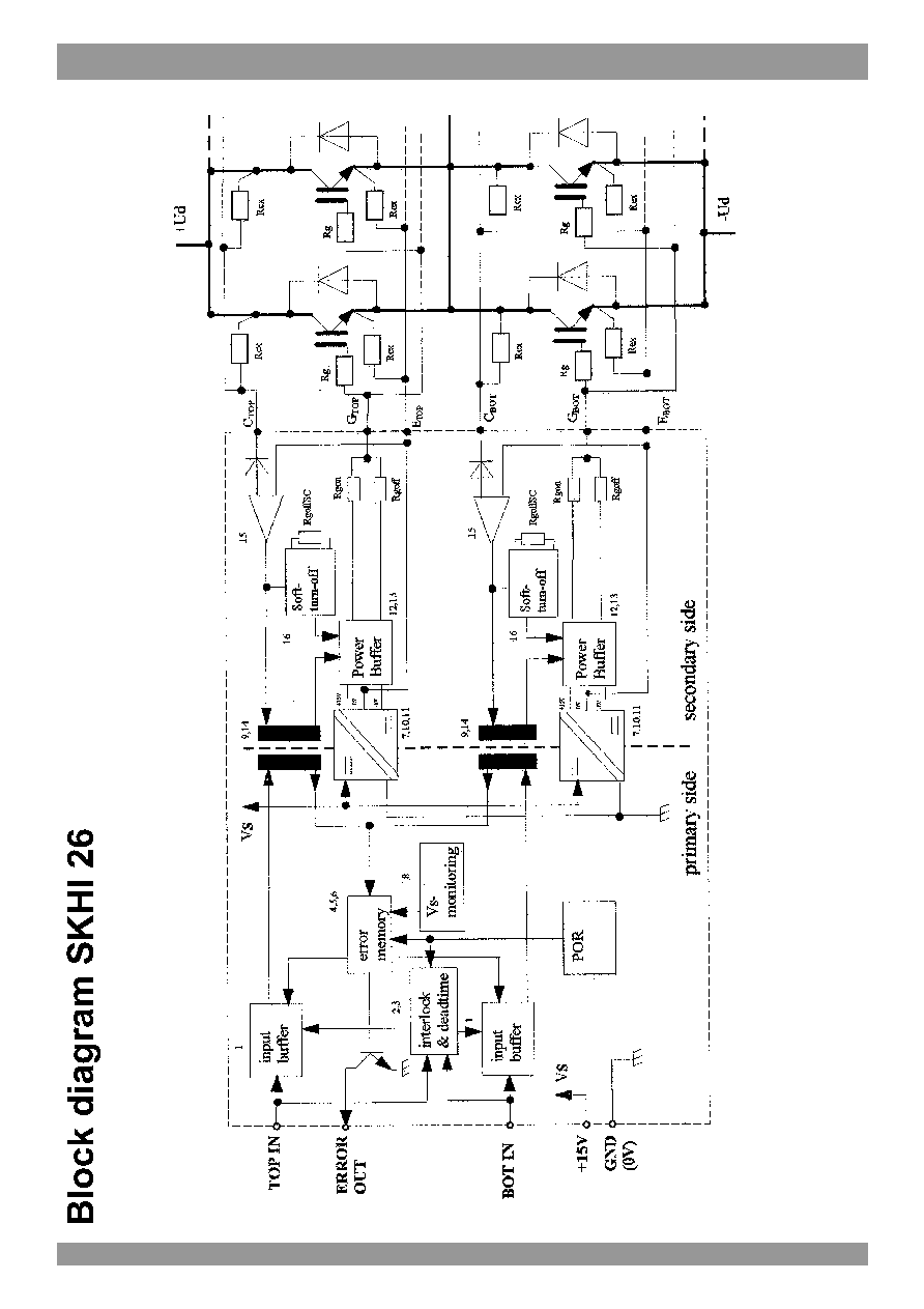
1
B
l
o
c
k
d
i
a
g
r
a
mm
of S
K
H
I 26
. T
he
num
ber
s
r
e
fer
to
des
c
r
i
p
ti
on
in
ch
apte
r
B. T
h
e po
wer
ou
tput
vo
lta
ge i
s
an e
x
a
m
pl
e o
f
IG
B
T
s
c
onn
ec
ted
in
par
al
le
l; t
he
max
i
m
u
m
num
ber
o
f
IG
BT
s
de
sp
end
s o
n
s
w
ic
ht
ing
fr
equ
enc
y
and
the
max
.
o
u
tpu
t
c
har
ge
per
p
u
ls
e.

1960
Driver Electronic ≠ PCB Drivers
26-01-2005
© by SEMIKRON
SKHI 26W, SKHI 26F
F
i
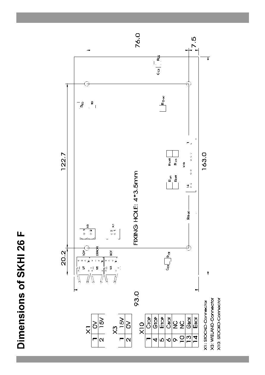
g. 2
P
osi
t
i
ons
of
the
ter
m
i
nal
s
(
v
ie
w ab
ov
e)
and
di
men
s
i
ons
(
i
n
mm
)
.

SKHI 26W, SKHI 26F
© by SEMIKRON 26-01-2005
Driver Electronic ≠ PCB Drivers
1961
F
i
g
.
3
P
o
s
i
t
io
ns
of
the t
e
r
m
i
nal
s (
v
ie
w fr
om
abo
ve
)
a
nd
dim
ens
io
ns
(
i
n
mm)
. T
h
e c
onn
ec
tor
s
X1
and
X3
ca
n be
us
ed
se
lec
t
i
v
e
.

1962
Driver Electronic ≠ PCB Drivers
26-01-2005
© by SEMIKRON
SKHI 26W, SKHI 26F
SEMIDRIVER SKHI 26W and SKHI 26F
High Power Double IGBT Driver
Technical Explanations
A. Properties and Functions of the Driver
1. The driver comprises short circuit protection for two
IGBTs in half bridge (pair of arms) connection. If a
single IGBT is driven, output TOP is to be used, and
the terminal C
BOT
of output BOT is to be connected to
terminal E
BOT
.
2. Short circuit protection is provided by measuring the
collector-emitter voltage. In case of short circuit the
soft turn-off circuit automatically increases the IGBT
turn-off time and hence reduces the DC voltage
overshoot.
3. The IGBTs are turned on by applying a positive
gateemitter voltage of 15 V, and turned off by a
negative gate-emitter voltage of - 8 V. In case of a
failure of the supply voltage the gate-emitter
connection is provided by a 10 k
resistor.
4. The driver also comprises the auxiliary power supplies
for the two boosters which are isolated by DC/DC
converters.
5. The two IGBTs of the half bridge are interlocked in
order to prevent them from being in the on-state
simultaneously. The locking time between the turn-off
signal for one IGBT and the release of the turn-on
signal for the other one is typically 3,3 µs (> t
doff
).
6. In the case of a short circuit both IGBTs are turned off
immediately. An error memory prevents the IGBTs
from being turned on again. The status of this memory
may be fed back to the control circuit via an open
collector transistor (SKHI 26 W) (error signal). The
error memory is only reset when both input signals are
zero.
7. The nominal voltage of the power supply V
S
is +15 V.
Its band of variation is from 14,4 to 15,6 V. The current
required is lower than 700 mA (conditions: 85 ∞C
temperature, V
S
= 15 V). Any undervoltage below
+13 V is monitored, and the IGBTs are turned off. An
error signal is released. Overvoltage is not monitored.
8. The switching signals are transmitted by isolating
pulse transformers. The isolation test voltages
2,5 kV
AC
.
The max. dv/dt rating between primary and secondary
side is 75 kV/µs.
9. The input and output signals are CMOS compatible,
for "W" version. The inputs have a Schmitt trigger
characteristic to suppress spurious pulses. The
thresholds of the inputs are
V
iT+
= min. 12,9 V
V
iT-
= max. 2,1 V
10. The operating temperature range is 0 ... + 70 ∞C.
Typ SKHI 26W: T
amb
= - 25 ∞C ... + 85 ∞C.
11. The typical delay times and propagation times for
signals are
Turn-on: 1,0 + t
TD
input to output
Turn-off: 1 µs
input to output
Error:
1 µs
error input to error signal output
12. In order to optimise the turn-on and turn-off speed
resistors are connected, but external resistors R
g
must
be added mainly for parallel connections, according to
the conditions of the given application. External
resistors R
g
, R
ex
and Rcx should be mounted on
additional circuit board near the paralleled modules.
The R
ex
assumes a value of 0,5
and its function is to
avoid the main current to circulate by the auxiliary
emitter which could make the emitter voltage against
ground unbalanced.
The R
cx
has a value of 47
and its function is to create
an average of V
CEsat
in case of short circuit for
V
CE
-monitoring (see Fig. 1).
13. The collectors of the IGBTs are connected to the driver
for monitoring the collector-emitter voltage V
CE
.
V
CEmax
= 1600 V. When paralleling modules, external
resistors R
cx
should be mounted on an additional
board near to the modules.
B. Description of the Circuit Block Diagram
The circuit block diagram (Fig. 1) shows the input on the
left and the output on the right.
The input side comprises the following components:
1. Input Schmitt trigger, CMOS compatible
In the "F" version we have the necessary optic input
buffers respectively ERROR output circuit, to perform
the optical and electrical signals.
2. Interlock circuit
The interlock circuit prevents the IGBT turning on
before the gate charge of the other IGBT is completely
discharged.
3. Short pulse suppression
The short pulse suppression makes sure that only
adequate trigger pulses are transmitted to the output
flip-flop.
4. Error monitoring
This circuit monitors pulses fed backwards via the
pulse transformers.
5. Inhibit pulse generator
In the error monitoring circuit, an inhibit pulse
generator discriminates between switching and error
signals. After any positive switching pulse edge the
error monitoring function is enabled. This is required
since the pulsetransformer causes a negative peak
voltage on its primary during re-magnetization. This
peak voltage would trigger the error monitoring without
the inhibit pulse.
6. Error memory
The error memory is triggered by the error monitoring
circuit. The error memory blocks the turn-on pulses to
both IGBTs simultaneously. Resetting is only possible

SKHI 26W, SKHI 26F
© by SEMIKRON 26-01-2005
Driver Electronic ≠ PCB Drivers
1963
when no pulses from the error monitoring are present
and both inputs are zero. The output signal is fed to a
terminal which is to be connected to the control circuit
(open-collector-transistor SKHI 26 W). An external
pull-up-resistor have to be provided on customers
control board.
7. DC/DC-Converter
It is the primary side control of the DC/DC converter for
transmitting the control power to the IGBTs.
8. Power supply monitoring
The supply voltage V
S
is monitored for its minimum
value of 13 V. If it falls below this value an error is
monitored and the turn-on pulses for the IGBTs are
blocked.
At initial switch-on the input pulses may only be
relea-sed more than 4 µs after the instant when V
S
has
reached its nominal value of 15 V.
The output comprises two drivers with the following
components:
9. Pulse transformer
It transmits the turn-on and turn-off signals for the
IGBT. In the reverse direction the error signal from the
V
CE
monitoring is transmitted via the same
transformer.
10. Power supply transformer for the DC/DC converter
11. Rectifier for the auxiliary power supply
12. Flip-flop
The flip-flop is pulse width triggered and is insensitive
to spurious pulses and high dv/dt values.
13. Drivers
The output transistors of the power drivers are
MOSFETs.
14. Reverse drivers for the pulse transformers
They transmit the signals from the VCE monitoring to
the pulse transformers.
15. V
CE
monitoring
It monitors the collector-emitter voltage V
CE
of the
IGBT during its on-state. V
CE
is limited internally to
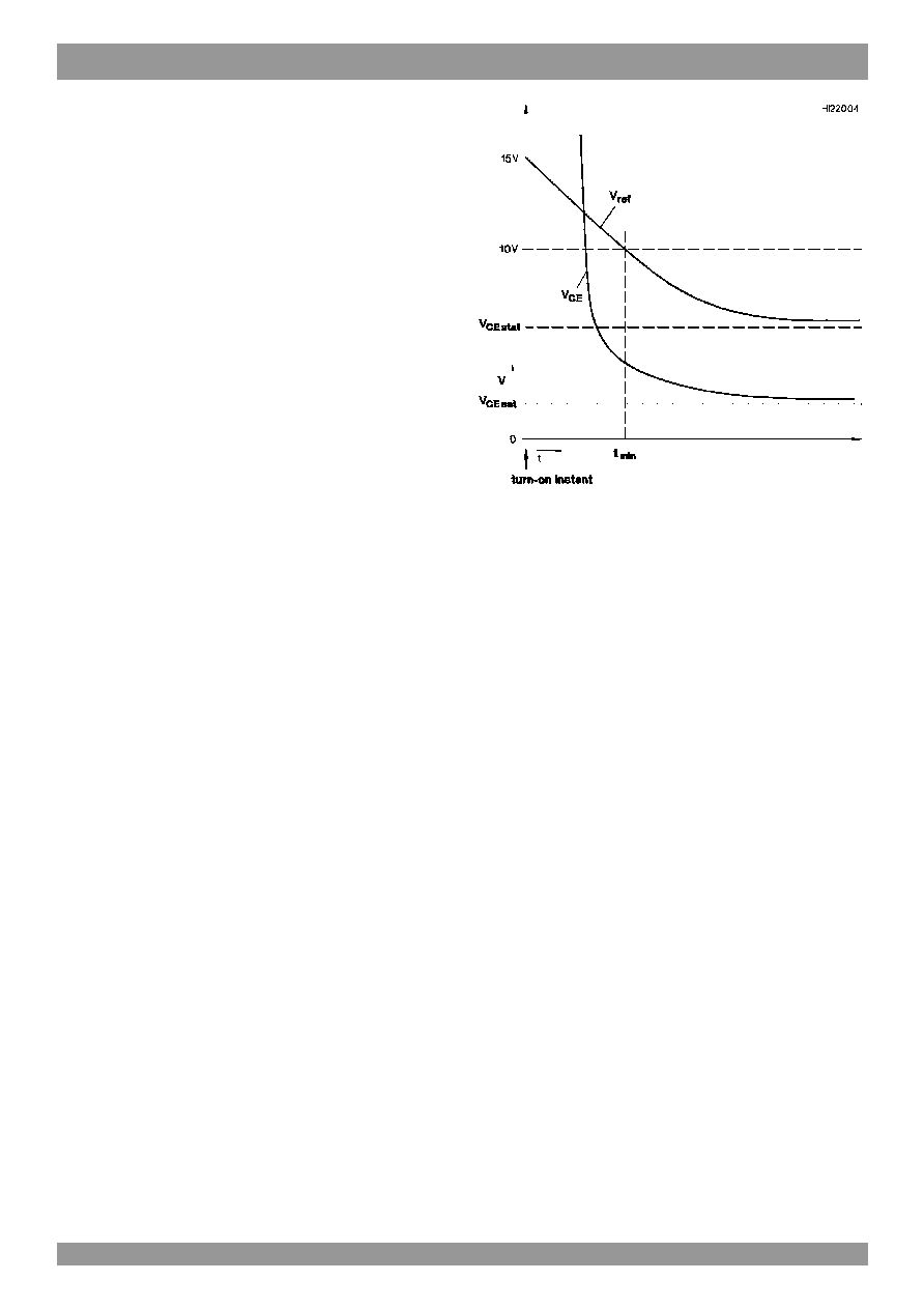
10 V (see fig. 4).
If the reference voltage V
CEref
is exceeded, the output
signal switches to zero. V
CEref
is dynamic. Immediately
after turn-on of the IGBT a higher value is effective
than in the steady state. When the IGBT is turned off,
V
CEref
is set to this higher value by the signal "reset".
Thesteady-state value V
CEstat
of V
CEref
is set for
standard IGBT (1200 V) values and has a typical value
of 5,2 V.
Fig.4 Waveform of the reference voltage V
CEref
of the V
CE
monitoring immediately after the turn-on signal for
the IGBT. A possible waveform of V
CE
is shown.
VCE is internally clamped to 10 V.
C. Application / Handling
1. The CMOS inputs of the driver are extremely
sensitiveto overvoltage. Voltages higher than (V
S
+
0,3 V) orunder - 0,3 V may destroy these inputs.
Therefore the following safety requirements are to be
observed:
- To make sure that the control signals do not
comprise overvoltages exceeding the above values.
- Protection against static discharges during handling.
As long as the driver is not completely assembled the
input terminals must be short circuited. Persons
working with CMOS devices should weara grounded
bracelet. Any floor coverings must notbe statically
chargeable. For transportation the input terminals
must be short circuited using, for example,
conductive rubber. Places of work must be
grounded.
The same safety requirements apply to the IGBTs.
2. The connecting leads between the driver and the
power module must be as short as possible.
For IGBT the leads should be twisted.
3. Any parasitic inductances should be minimized.
Overvoltages may be damped by C or RCD snubber
net-orks between the main terminals of the power
module.
4. When first operating a newly developed circuit, low
collector voltage and load current should be used in
the beginning, and these values should be increasod
gradually, observing the turn-off behaviour of the
freewheeling diodes and the turn-off voltage spikes
across the IGBT by means of the oscilloscope. Further
the case temperature of the power module should be
monitored.
When the circuit works correctly, short circuit tests can
be made, starting again with low collector voltage.
5. lt is important to feed any errors back to the control
circuit and to switch the equipment off immediately in
such events. Repeated turn-on of the IGBT into a short
circuit with a frequency of several kHz may destroy the
device.

