 | –≠–ª–µ–∫—Ç—Ä–æ–Ω–Ω—ã–π –∫–æ–º–ø–æ–Ω–µ–Ω—Ç: SKHIBS01 | –°–∫–∞—á–∞—Ç—å:  PDF PDF  ZIP ZIP |
© by SEMIKRON
020826
B 14 ≠ 33
SKHIBS 01
Absolute Maximum Ratings Ta = 25 ∞C
Symbol Term
Value
Units
V
S
V
IH
V
CE
dv/dt
V
isol IO
T
op
/ T
stg
Supply Voltage primary
Input signal Voltage High
(5 V input level)
Collector-Emitter-Voltage
Rate of rise and fall of voltage
(secondary to primary side)
Isol. test voltage IN-OUT (2 sec. AC)
Operation Temp.
Storage Temp.
15,6
6.5
1200
15
2500
0 ... + 70
1)
0 ... + 70
1)
V
V
V
kV/ms
V
∞C
∞C
Sixpack Circuit
I
OUT peak
I
OUTAV
f
sw
R
IN
R
gmin
Q
OUT/pulse
Output peak current
Output average current (max)
Switching frequency (max)
Input resistance
Minimum gate resistor
Charge per pulse
1,5
15
20
500
18
8)
0.750
A
mA
kHz
W
W
mC
Brake Chopper Circuit
I
OUT peak
I
OUTAV
R
IN
f
sw
R
gmin
Q
OUT/pulse
T
TRIPBRC
2)
Output peak current
Output average
Input resistance
Switching frequency (max)
Minimum gate resistor
Charge per pulse
Triplevel temp.-monitoring
1
8,4
500
20
15
0.42
115 ± 5
3)
A
mA
W
kHz
W
mC
∞C
Electrical Characteristics T
a
= 25 ∞C
Symbol
Term
min
typ
max
Units remark
V
S
Supply voltage primary
14.4
15.0
15.6
V
Pin 11
I
S
Supply current max
0.43
A
I
SO
Supply current primary standby
0,165
A
V
iH5V
4)
Input voltage 5 V input level
5
V
V
iH15V
4)
Input voltage 15 V input level
15
V
Rv=1k
V
iInhibit off
Inhibit voltage off
< 5
V
Sixpack Circuit
V
G(on)
Turn-on gate voltage
+ 15
V
V
G(off)
Turn-off gate voltage
- 8
V
t
d(on) IO
Input-Output turn-on
propagation time
0.3
ms
t
d(off) IO
Input-Output turn-off
propagation time
0.3
ms
Brake Chopper Circuit
V
G(on)
Turn-on gate voltage
+ 15
V
10 mA
V
G(off)
Turn-off gate voltage
0
V
V
GESTAT
Reference voltage for
V
CE
-monitoring
5,3
V
V
OL
5)
logic low output voltage
500
mV
V
OH
5)
logic high output voltage
30
V
t
d(on) IO
Input-Output turn-on
propagation time
3.9
ms
t
d(off) IO
Input-Output turn-off
propagation time
6.4
ms
t
d(err) Gate
6)
Error input-output
propagation time
3.2
ms
V
CEBRC
t
d(err) ovr
7)
Error input-output
propagation time
6.7
ms
SEMIDRIVER
Æ
IGBT Driver kit
SKHIBS 01
Preliminary Data
General Features
W
driver for sixpack and sevenpack
up to V
CES
= 1200 V
W
used together with the
transformer
W
Inhibiting signal
W
ERROR output (open collector
transistor)
Sixpack circuit
W
input signals transferred
via opto couplers
W
turn on voltage + 15 V /
turn off voltage - 8 V
W
separate, insulated supply
voltage for the 3 TOP switches
W
common, insulated supply
voltage for the 3 BOT switches
brake chopper circuit
W
driver for BRC - IGBT
W
V
CE
monitoring for brake chopper
IGBT
W
temperature monitoring
(external adjustable)
for BRC - IGBT
W
turn on voltage + 15 V /
turn off voltage 0 V
W
isolation via opto couplers
1)
- 25 ∞C ... + 85 ∞C on request
2)
If temperature monitoring in use
Trip level can be adjusted with an
external resistor
3)
factory adjusted
4)
R
in
= 500 W
5)
open collector output, external pull-
up resistor
6)
time for shut off the gates when
failure occur
7)
time between failure occur and
information available at output
ERROR (Pin 8)
8)
at 20 kHz switching frequency
B 14 ≠ 34
020826
© by SEMIKRON
SKHIBS 01
Sixpack circuit
+ brake chopper circuit
SEMIDRIVER
Æ
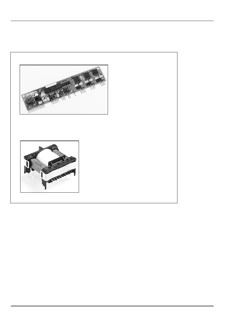
SKHIBS Driver kit
Subprints for soldering into a printed circuit board
Preliminary Data
VXESULQW
transformer
SKHIBS 01
Overview SEMIKRON driver SKHIBS 01
The SEMIKRON driver kit SKHIBS consists of 1 subprint and 1 transformer, which have to be soldered into a printed
circuit board (PCB).
Subprint together with the transformer can be used for driving max. 7 IGBTs, e.g. a sixpack or a sixpack with brake
chopper.
SKHIBS drives IGBTs up to V
CES
=1200 V. The output capability was designed to drive 120 A IGBTs up to 20 kHz.
The power supply for the driver kit may be the same used for the control board (15 V ± 0.6 V), without the requirements
of insulation. The signals (inverter) between primary side and secondary side are transmitted via opto couplers (also
used for insulation) with a dv/dt > 15 kV/msec.
Operation (storage) temperature is from 0 ∞C to + 70 ∞C, (- 25 ∞C to + 85 ∞C on request).
To protect the subprints against moisture and dust they are coated with varnish.
© by SEMIKRON
020826
B 14 ≠ 35
SKHIBS 01
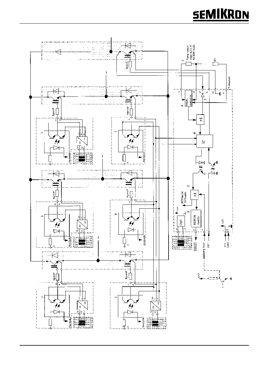
SKHIBS 01 Block Diagram
B 14 ≠ 36
020826
© by SEMIKRON
SKHIBS 01
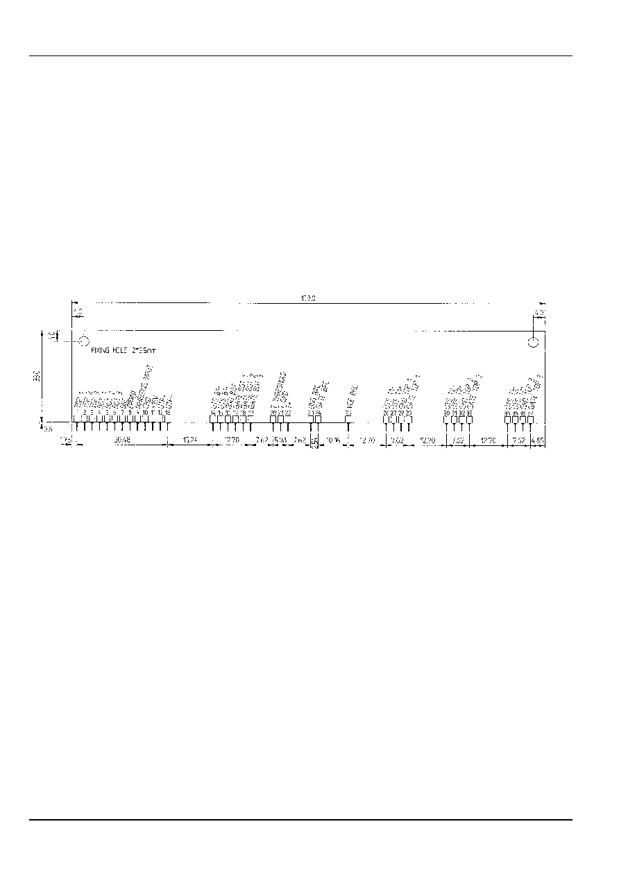
Outline subprint
Description of the circuit block diagram SKHIBS 01
The circuit shows the minimal configuration for driving 6 inverter IGBTs and 1 brake chopper IGBTs.
The transformer delivers the insulated supply voltage for driving the IGBTs.
The regulation of these voltages is made on the subprint.
For each TOP IGBT + 15 V is used for switching on the IGBT,
- 8 V is used for switching off the IGBT.
The BOT IGBTs are supplied with one common power supply, + 15 V is used for switching on and - 8 V is used for
switching off. The brake chopper IGBT is supplied due to the power supply used for the BOT switches.
For switching off the brake chopper IGBT 0 V is used. Switching on is made with + 15 V.
The driver kit SKHIBS 01 is able to drive SEMIKRON IGBTs up to I
C
= 120 A specified at 25 ∞C.

© by SEMIKRON
020826
B 14 ≠ 37
SKHIBS 01
Characteristics
PIN
symbol
term
remark
1
TOP 1
input TOP 1
5 V / 10 mA (using 15 V input voltage; additional Rv = 1 kW necessary
2
TOP 2
input TOP 2
5 V / 10 mA (using 15 V input voltage; additional Rv = 1 kW necessary
3
TOP 3
input TOP 3
5 V / 10 mA (using 15 V input voltage; additional Rv = 1 kW necessary
4
BOT 1
input BOTTOM 1
5 V / 10 mA (using 15 V input voltage; additional Rv = 1 kW necessary
5
BOT 2
input BOTTOM 2
5 V / 10 mA (using 15 V input voltage; additional Rv = 1 kW necessary
6
BOT 3
input BOTTOM 3
5 V / 10 mA (using 15 V input voltage; additional Rv = 1 kW necessary
7
BRC
input brake chopper
5 V / 10 mA
8
ERROR
output ERROR
open collector transistor (30 V / 10 mA)
9
Inhibiting Input Inhibit signal
connected to open collector (max. 15 V)
10
GND
GND power supply
controlled power supply
11
+ 15 V
+ 15 V power supply
controlled power supply (15 V+ / -0.6 V)
12
ÐTP +
input voltage DC/DC converter
connected to PIN 1 transformer short distance for connection to transformer required
13
ÐTP -
input voltage DC/DC converter
connected to PIN 2 transformer short distance for connection to transformer required
14
ÐTS B1-
input voltage BOT DC/DC converter
connected to PIN 8 transformer short distance for connection to transformer required
15
ÐTS B1+
input voltage BOT DC/DC converter
connected to PIN 7 transformer short distance for connection to transformer required
16
GND BOT
GND BOT 1 - 3
17
Gate BOT 1
output gate BOT 1
turn on + 15 V, turn off - 8 V
18
Gate BOT 2
output gate BOT 2
turn on + 15 V, turn off - 8 V
19
Gate BOT 3
output gate BOT 3
turn on + 15 V, turn off - 8 V
20
T
THRESHOLD
input threshold voltage T
BRC
adjustable due to external resistor R1
21
T GND
GND for PIN 20 and 22
22
T +
input temperature sensor
connected to BRC-Temp. sensor used in SEMIKRON devices MiniSKiiP 8
23
GND BRC
GND BRC
24
Gate BRC
output gate BRC
turn on + 15 V, turn off 0 V
25
VCE BRC
VCE monitoring BRC
connected to collector BRC- IGBT
26
ÐTS T1-
input voltage TOP 1 DC/DC converter connected to PIN 10 transformer short distance for connection to transformer required
27
ÐTS T1+
input voltage TOP 1 DC/DC converter connected to PIN 9 transformer short distance for connection to transformer required
28
GND TOP 1
GND TOP 1
29
Gate TOP 1
output gate TOP 1
turn on + 15 V, turn off - 8 V
30
ÐTS T2-
input voltage TOP 2 DC/DC converter connected to PIN 12 transformer short distance for connection to transformer required
31
ÐTS T2+
input voltage TOP 2 DC/DC converter connected to PIN 11 transformer short distance for connection to transformer required
32
GND TOP 2
GND TOP 2
33
Gate TOP 2
output gate TOP 2
turn on + 15 V, turn off - 8 V
34
ÐTS T3-
input voltage TOP 3 DC/DC converter connected to PIN 14 transformer short distance for connection to transformer required
35
ÐTS T3+
input voltage TOP 3 DC/DC converter connected to PIN 13 transformer short distance for connection to transformer required
36
GND TOP 3
GND TOP 3
37
Gate TOP 3
output gate TOP 3
turn on + 15 V, turn off - 8 V
PIN-array subprint

B 14 ≠ 38
020826
© by SEMIKRON
SKHIBS 01
Before giving detailed informations about SKHIBS 01 a short description is given about the using of the subprint and the
transformer.
a)
Subprint together with the transformer describes the minimal configuration for driving 6 IGBT switches and 1 brake
chopper IGBT. 6 Opto couplers are used for driving the IGBTs of the inverter circuit.
Driving of the brake chopper IGBT is made with an integrated circuit, which allows the short circuit protection of
this brake chopper IGBT due to V
CE
-monitoring. The protection of the brake chopper against overtemperature, e.g.
using the temperature sensor e.g. in MiniSKiiP 8 devices, can also be made.
b)
The transformer supplies the insulated supply voltage. The 6 IGBT for the inverter are supplied with regulated
+ 15 V for switching on and -8V for switching off the IGBTs.
The 3 TOP-IGBTs have separate supply voltages. The 3 BOT-IGBTs have a common supply voltage.
This voltage is also used for driving the brake chopper IGBT, if in use.
Circuits on subprint provide the regulated voltages for switching the IGBTs.
c)
SKHIBS 01 has no feature to protect the IGBTs against short circuit. But with the input PIN 9 ,,INHIBITING INPUT"
all inverter IGBTs can be made inactive, when the customers evaluation electronic delivers a fault signal, e.g. in
short circuit condition.
d)
The brake chopper IGBT of the subprint has a separate input PIN 7 ,,BRC" for externally controlling of this IGBT
in chopper mode.
2.
Input circuit for inverter
The signal transfer to each IGBT is made with opto-couplers, used for switching on and switching off the IGBT.
When using 5 V inputsignal (TTL-logic), no additional resistor in series to the input is necessary.
Using positive 15 V input voltage an additional resistor R
v
= 1 kW have to be connected in series to the inputs.
Because no interlock of TOP and BOT switch in each halfbridge is made on the subprint, the controller
have to provide this interlock. Deadtime of interlock should be t
TD
> 3 msec.
Please observe:
No interlock will destroy the IGBT when switching.
There are no gate resistors Rgon/off provided on the subprint.
The max. output peak current IOUTpeak < 1,5 A have to considered, when fixing the gate resistors.
The minimum permissible gate resistor is Rg = 18 W. 18 kHz < f
sw
< 20 kHz
15 W. 16 kHz < f
sw
< 18 kHz
12 W < 16 kHz switching frequency
3.
INHIBITING signal
Therefore the SKHIBS 01 has no protection against short circuit it will be possible to disconnect the low voltage
side from high voltage side in case of a fault condition due to the input PIN 9 ,,INHIBITING INPUT". In case of
fault condition the INHIBITING INPUT signal have to be turned to LOW signal (set to GND).
When the INHIBITING signal is short in time, an internal circuit extent a short pulse to 1 ms.
The INHIBITING signal sets the ERROR output PIN 8 from LOW to HIGH level.
The power supply for the inverter IGBTs as well as the brake chopper IGBT, will also be disconnected, when the
brake chopper IGBT driver circuit creates an ERROR signal caused either due to VCE-monitoring or
overtemperature monitoring of the brake chopper IGBT.
4.
ERROR monitoring
The Error output PIN 8 ,,ERROR" is an open collector transistor (max. 30 V / 10 mA).
In case of an ERROR (either external fault information via the input PIN 9 ,,INHIBITING INPUT" or because of an
Features of subprint
1. Introduction

© by SEMIKRON
020826
B 14 ≠ 39
SKHIBS 01
internal fault information (created on subprint) the ERROR output PIN 8 is set to HIGH level.
When there is a fault condition, transferred due to the INHIBITING INPUT signal, the ERROR output is active until
the INHIBITING INPUT is > 5 V (Umax. = + 15 V).
When PIN 8 ,,ERROR" is active due to the V
CE
-monitoring or overtemperature sensing of the brake chopper, the
ERROR output is active until the input signal PIN 7 ,,BRC" is set to LOW level (OV) for t > 1msec.
5.
brake chopper driver
The brake chopper driver IC transfers the on and off signals to the brake chopper IGBT.
Switching on of the IGBT is made with + 15 V, switching off is made with 0 V.
This IC also monitors the V
CE
-voltage of the brake chopper. If there is a short circuit, the V
CE
-monitoring delivers
a error signal at PIN 8 "ERROR" when the voltage exceed typ. 5.3 V.
When the brake chopper is not in use, input PIN 7 ,,BRC" have to be set to ,,GND" (PIN 10).
Also the input on secondary side PIN 25 ,,V
CE
BRC" have to be connected to ,,GND" (PIN 23).
Temperature monitoring (Brake chopper only)
Also an ERROR signal will be transferred to the ERROR output PIN 8 ,,ERROR", when the temperature exceeded
a value, fixed by the customer (factory adjusted: max. T
TRIP
= 115 ∞C + / - 5 ∞C).
This circuit evaluates the overtemperature of a thermal resistor type KTY 85 (Philips), which is soldered on the
DCB ceramic of SEMIKRON MiniSKiiP 8 devices.
When this temperature is not in use, input PIN 21 ,,T GND" have be connected to PIN 22 ,,T+".
Factory adjusted the overtemperature detection is fixed to 115 ∞C heatsink temperature.
Due to the paralleling of the external resistor R1 between PIN 20 ,,T THRESHOLD" and PIN 21 ,,GND" the
threshold level can be adjusted, according to the following table.
Table 2: trip level for temperature protection; accuracy = + / - 5 ∞C
Ttrip heatsink
calculated resistor R1
recommended resistor R1 (E96)
50 ∞C
3.54 kW
3.57 kW
60 ∞C
4.41 kW
4.42 kW
70 ∞C
5.69 kW
5.62 kW
80 ∞C
7.70 kW
7.68 kW
85 ∞C
9.22 kW
9.31 kW
90 ∞C
11.38 kW
11.30 kW
95 ∞C
14.66 kW
14.70 kW
100 ∞C
20.26 kW
20.50 kW
105 ∞C
31.98 kW
31.60 kW
110 ∞C
70.19 kW
69.80 kW
B 14 ≠ 40
020826
© by SEMIKRON
SKHIBS 01
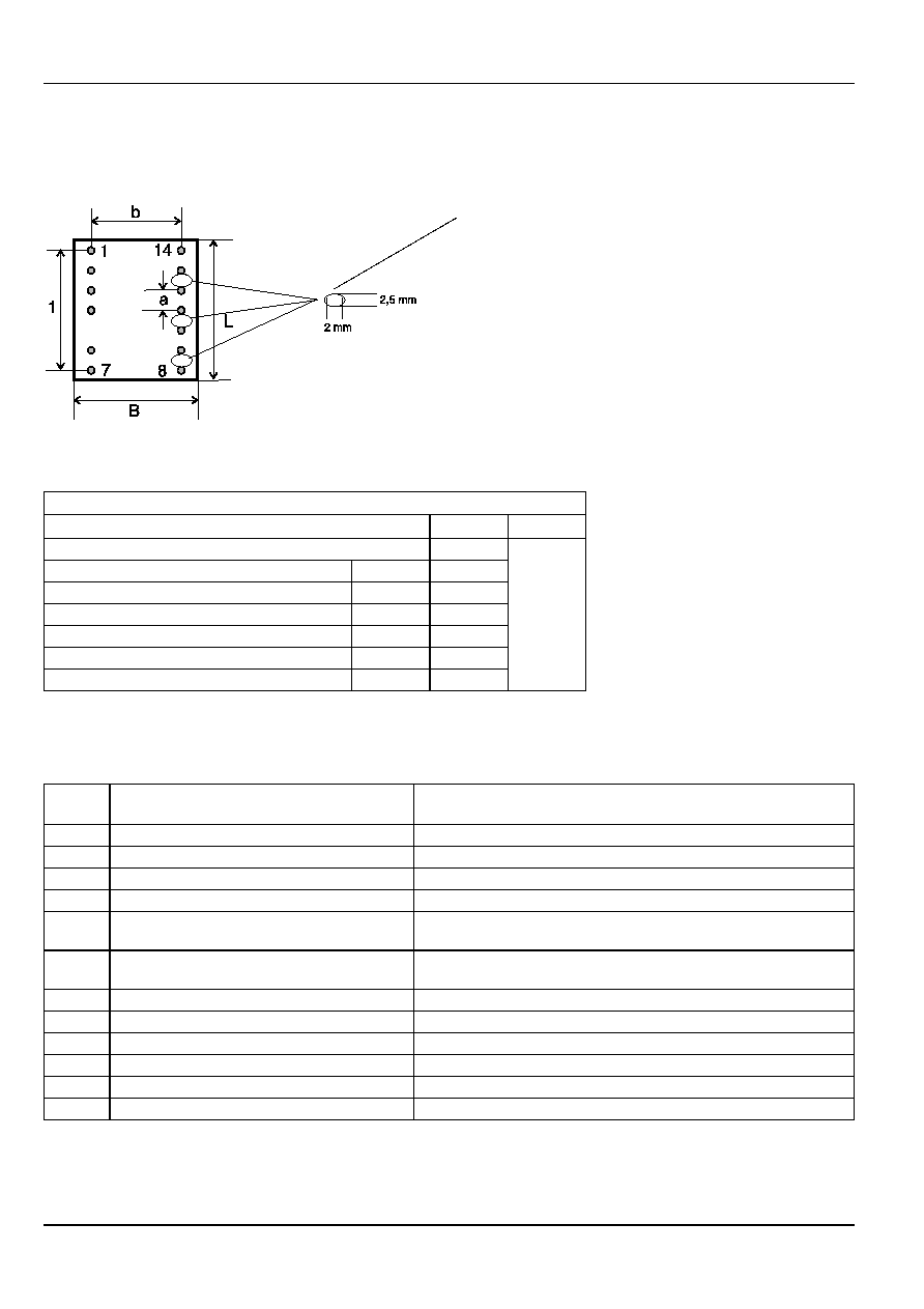
Dimensions
term
value
unit
PIN dimension
QU. 0.7
mm
length
L
35.4
width
B
31.4
height
H
< 25
distance between pins
a
5.08
distance between pins lines
b
22.86
distance between pins 1 to 7 and pins 8 to 14
i
30.48
Transformer
Preliminary Data
Fig. 3 Outline transformer
PIN array
PIN
number
term
remark
1
supply voltage (+ 15 V / 0 V)
connected to PIN 12 subprint (short distance for connection required)
2
supply voltage (+ 15 V / 0 V)
connected to PIN 13 subprint (short distance for connection required)
3
reserved
4
reserved
7
output voltage II
(used for supply of BOT switches)
connected to PIN 15 subprint (short distance for connection required)
8
output voltage II
(used for supply of BOT switches)
connected to PIN 14 subprint (short distance for connection required)
9
output voltage III (used for supply of TOP 1)
connected to PIN 27 subprint (short distance for connection required)
10
output voltage III (used for supply of TOP 1)
connected to PIN 26 subprint (short distance for connection required)
11
output voltage IV (used for supply of TOP 2)
connected to PIN 31 subprint (short distance for connection required)
12
output voltage IV (used for supply of TOP 2)
connected to PIN 30 subprint (short distance for connection required)
13
output voltage V (used for supply of TOP 3)
connected to PIN 35 subprint (short distance for connection required)
14
output voltage V (used for supply of TOP 3)
connected to PIN 34 subprint (short distance for connection required)
Holes on PCB may be necessary due
to clearance and creepage distance
This technical information specifies devices but promises no characteristics. No warranty or guarantee expressed or implied is made
regarding delivery, performance or suitability.