1976
Driver Electronic ≠ PCB Drivers
23-02-2004
© by SEMIKRON
SKHIT 01 ...
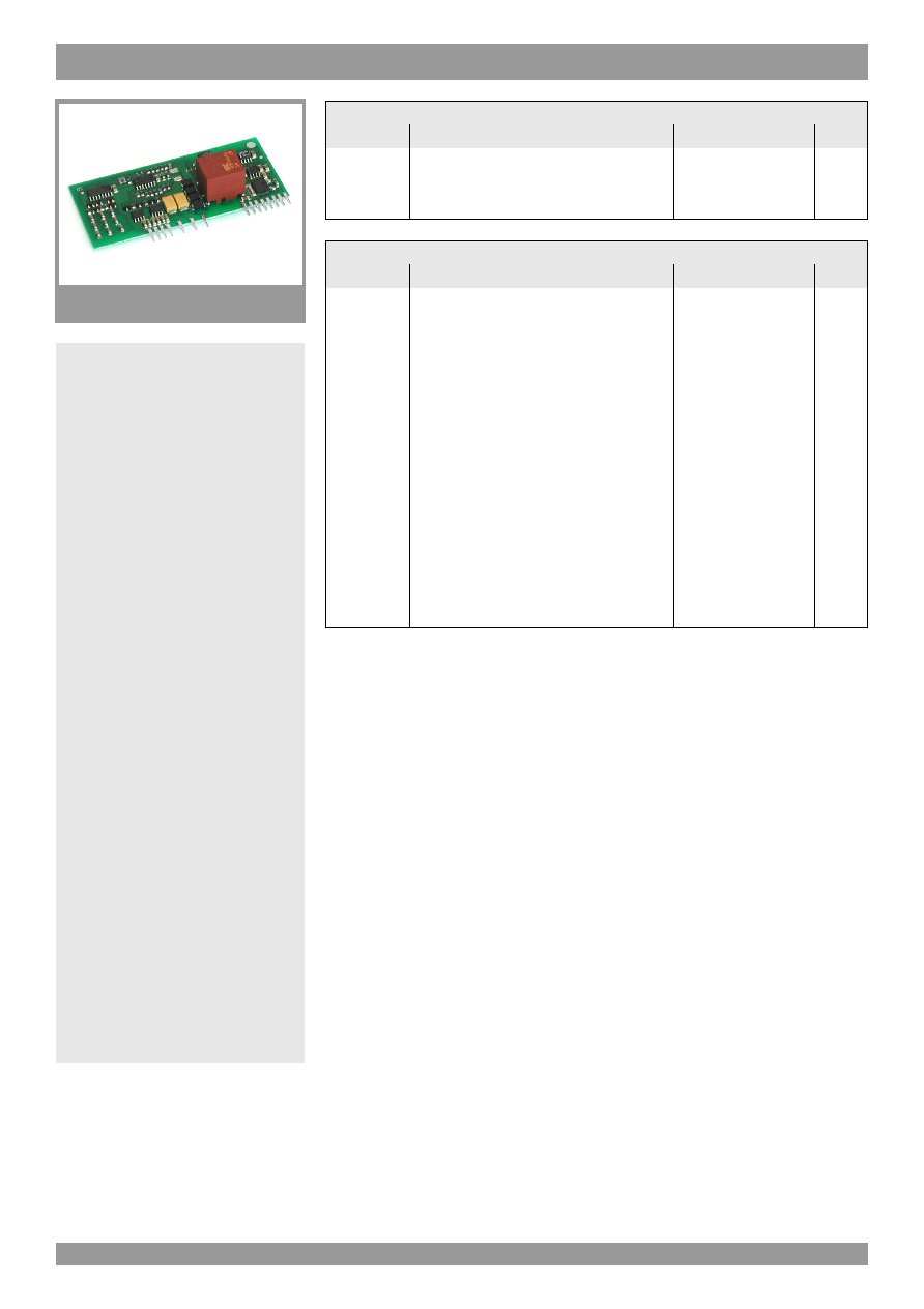
SEMIDRIVER
TM
Thyristor driver for three
phase half controlled
bridge
SKHIT 01
Preliminary Data
Features
∑ patent DE 197 10 371
∑ SKHIT 01 can be soldered
directly onto a printed circuit
board
∑ Isolation by transformers (DC/
DC) and opto couplers (signal)
Typical Applications
∑ DC-link voltage converter with
precharge circuit
Absolute Maximum Ratings
T
a
= 25 ∞C, unless otherwise specified
Symbol
Conditions
Values
Units
Isolation test voltage
2500
V
input - output (2 sec. AC)
Operating temperature
0 ... + 60
∞C
Storage temperature
- 25 ... + 70
∞C
Characteristics
T
a
= 25∞C, unless otherwise specified
Symbol
Conditions
min.
typ.
max. Units
Operating voltage (phase to phase)
480
528
V
Trigger current (output)
400
mA
Trigger current pulse length
10
12
15
µs
Pulse current cycling frequency
6,6
8,3
10
kHz
Power supply
Supply voltage
14,4
15
15,6
V
Supply current (standby)
60
mA
Supply current (max.)
150
mA
Signals
Thyristor trigger enable threshold (HIGH)
3,9
5,5
V
Thyristor trigger enable threshold (LOW)
-0,5
1
V
Input current "On"
10
mA
Open collector error output (error = Low)
U
CE
(I
C
= 4 mA)
1
V
I
C
5
mA
Maximum rating voltages
Power to earth (overvoltage cat. III)
300
V
eff
Power to logic (overvoltage cat. II)
900
V
eff
Logic to earth
60
V
eff
1978
© by SEMIKRON
SCR / Thyristor Trigger Module
SKHIT 01
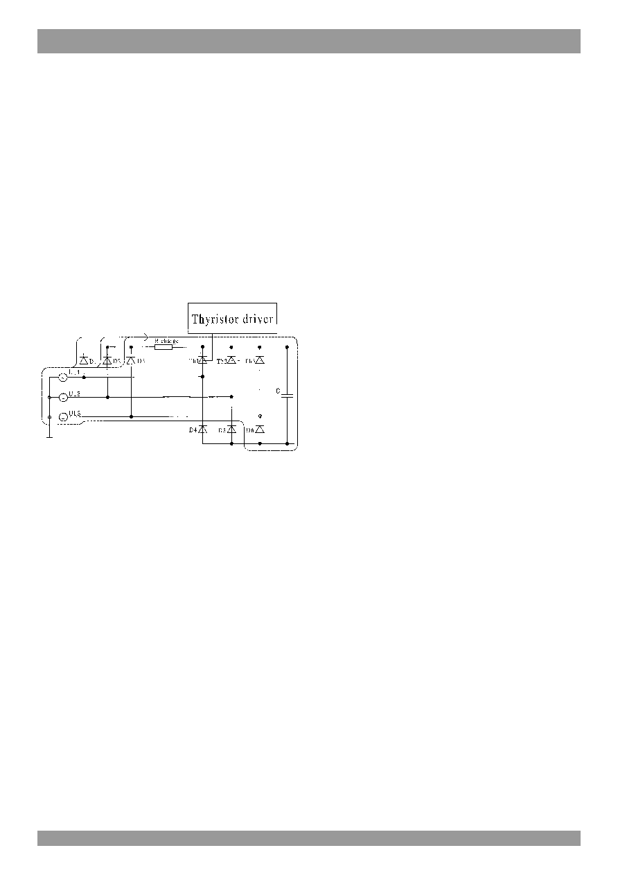
The SCR / thyristor trigger module SKHIT 01 has been
designed for triggering half controlled bridges.
Application range
When switching on a DC-link voltage converter the
DC-link capacitors are uncharged and are, thus,
signalizing a short circuit situation to the applied supply
voltage. Therefore, the charge current has to be limited to
the rated value by switching suitable circuits; SEMIKRON
prefers to realize those circuits without electromagnetic
components such as relays or contactors. Instead of an
uncontrolled B6-diode input bridge (B6U), a half-controlled
diode thyristor bridge is used (B6H).
Fig. 3 Charge circuit
At the beginning of the switch-on process the thyristors
are blocked, the DC-link capacitors are charged via diodes
D1
- D3 and R
charge
(fig. 3). After having finished the
charging process, the thyristors have permanently to be
triggered by a driver stage such as the SKHIT 01.
Technical explanations
Conventional thyristor drivers use to trigger the thyristors
in synchronization with the line voltage, i.e. the trigger
signal is given out at a (variable) phase angle of the line
voltage. However, such an angle control is only necessary
for controlling the rectifier output voltage.
The SKHIT 01 fades out the trigger pulses at negative
thyristor voltage.
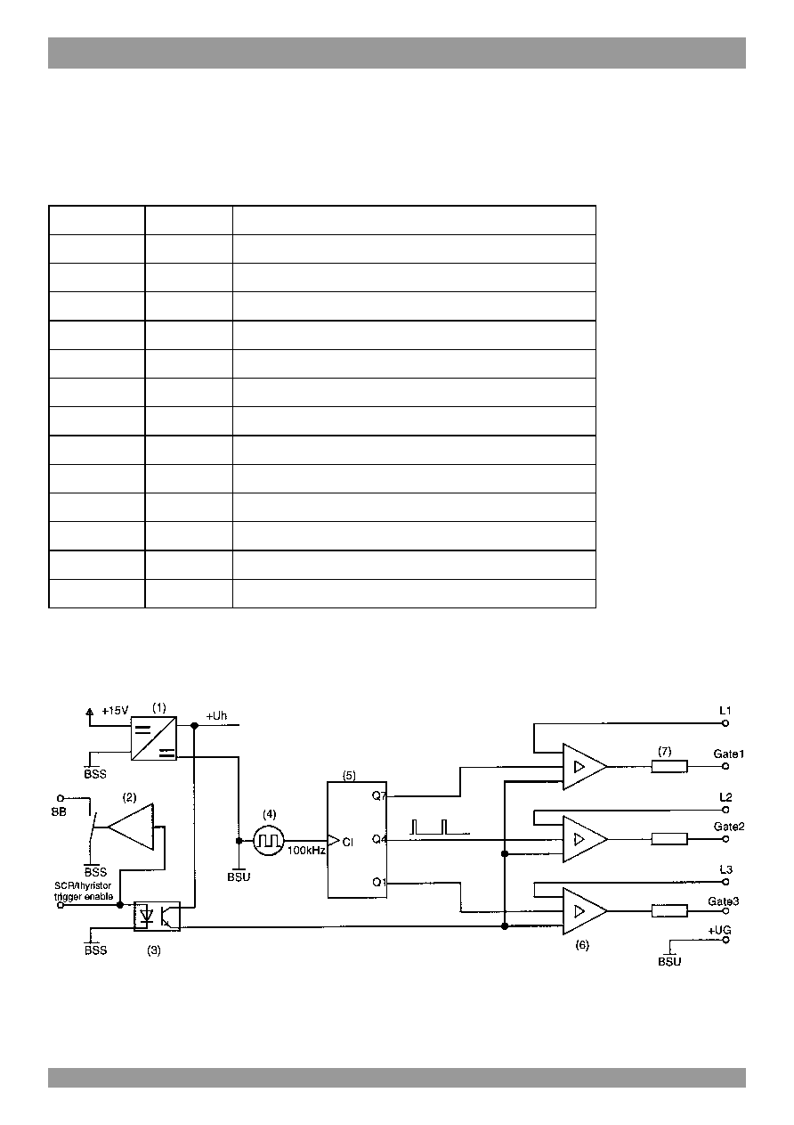
Description of the block diagram (Fig. 1)
A cycle generator (4) and a decimal counter (5) generate
square-wave signals, which are to each other
time-delayed with a cyclic duration factor of 10µs and a
frequency of 10kHz. These pulses are directed to the
single thyristor gates via comparators and output
amplifiers (6) as well as series resistors (7). If the voltage
applied to the thyristor is negative or if there is no release
signal, the trigger pulse signals will be suppressed. The
phase relationship of the driver pulses is independent of
the phase relationship of the line voltage.
The trigger enable signal (THO) is transmitted to the
process logic via an optocoupler (3).
The ground connection of the control logic of an inverter is
not identical with the ground connection of the thyristors.
The ground connection potential of the secondary circuit
of the thyristor trigger stage (BSU) is identical with the
positive rectifier output voltage "+UG", while the input
ground connection potential normally is identical with the
logic potential "BSS". The required supply voltage is
transmitted via a DC/DC-converter (1).
The feedback signal "ready for operation" (BB) is set to
LOW, if the thyristor trigger enable signal is not applied
(THO=Low).
Mounting instructions
∑ The SKHIT 01 thyristor driver has been designed for
vertical mounting (soldering) to PCBs.
∑ The driver should be placed as close as possible to the
thyristors.
∑ The necessary creepage paths on the PCB have to be
dimensioned according to the application-specific
voltage ratings.
Further application notes
The PCB-mountable thyristor driver SKHIT 01 is delivered
as a subcomponent for a driving system dimensioned by
the user. The responsibility for proper system operation,
especially with view to keeping the valid standards, is
taken only by the user.
This technical information specifies devices but promises no characteristics. No warranty or guarantee expressed or
implied is made regarding delivery, performance or suitability.