 | –≠–ª–µ–∫—Ç—Ä–æ–Ω–Ω—ã–π –∫–æ–º–ø–æ–Ω–µ–Ω—Ç: SKIC2001A | –°–∫–∞—á–∞—Ç—å:  PDF PDF  ZIP ZIP |
© by SEMIKRON
0699
1
I
:
\
M
AR
KETIN\
F
RA
MED
AT\
datbl\
Treiber\Sk
i
c
2001AB
.
fm
Absolute Maximum Ratings (T
a
= 25 ∞C)
Symbol Term
Values
Units
V
DD15V
V
DD12V
V
DD5V
V
IH
V
IL
f
sw
T
op
/ T
stg
15 V supply voltage (SKIC 2001 A)
12 V supply voltage (SKIC 2001 B)
5 V supply voltage
(reference for input signals)
input signal voltage (HIGH) max.
input signal voltage (Low) min.
switching frequency
operating/storage temp.
18
15
6
V
DD5V
+ 0,3
GND - 0,3
50
≠ 25 ... + 85
V
V
V
V
V
kHz
∞C
Electrical Characteristics (T
a
= 25 ∞C)
1)
Symbol
Term
Values
Units
V
DD15V
V
DD12V
V
DD5V
V
BAND-
GAP
I
S5V
I
S15V
t
d
15 V supply voltage (SKIC 2001 A)
12 V supply voltage (SKIC 2001 B)
5 V supply voltage
reference voltage 10 V
supply current (V
DD5V
); typ
4)
supply current (V
DD15V
); typ
4)
propagation time
15 + 5 %
12 + 5 %
5 + 5 %
9,99 ... 10,01
3
15
960
V
V
V
V
mA
mA
ns
t
TDswitch
2)
dead time of interlock; typ.
0,
1,
2,
3,
4
µ
s
t
supswitch
t
supreset
V
SU
V
SU 5 V
short pulse suppression
TOP-
BOT
;typ
pulses are suppressed
pulses are not suppressed
short pulse supppression RESET;
typ.
supply undervoltage monitoring
using V
DD15V
SKIC 2001 A
using V
DD12V
SKIC 2001 B
supply undervoltage monitoring
using V
DD5V
< 480
3)
> 640
9
13,0
10,0
3
ns
ns
µ
s
V
V
V
input signal TOP, BOTTOM, SELECT, TDT1, TDT2
V
it+
V
iT-
R
down
R
UP
input threshold voltage (High) min
input threshold voltage (Low) max
internal pull down resistor (TOP;
BOTTOM)
internal pull up resistor (SELECT,
TDT1, TDT2)
3,5 - 3,9
1,5 - 2,0
66 + 2
64 + 2
V
V
k
k
ERROR input signals TOPERR, BOTERR
V
ET+
V
ET-
R
EUp
t
swOSZ
t
Td
input threshold voltage (High)
input threshold voltage (LOW)
internal pull up resistor
oszillator frequency DC/DC-conv.
time of interlock DC/DC-converter
> 3,55
< 1,3
27 + 0,2
500
3)
250
V
V
k
kHz
ns
ERROR input signal SENSEERR
V
ET+
V
ET-
R
EUp
input threshold voltage (High)
input threshold voltage (LOW)
internal pull up resistor
3,4 + 0,2
2,2 + 0,2
36 + 2
V
V
k
output signal ERROR; TPW, TW
I
outmax
max. output current at V
DD5V
+ 5
mA
V
outmax
max. output voltage at + 5 mA
4,8
V
V
outmin
min. output voltage at - 5 mA
0,22
V
output signal TOPOUT; BOTOUT; TR1P; TR1N; TR2P; TR2N
r
Ti
t
r
typ.
t
f
typ.
inhibit time for V
CE; ERR
rise time
fall time
2
25
5)
35
5)
µ
s
ns
ns
SEMIDRIVER
Æ
IGBT Driver Circuit
SKIC 2001 A
SKIC 2001 B
Preliminary Data
Features
IGBT-halfbridge driver circuit with
protection functions
∑
Interlock of TOP and BOTTOM
switches of one halfbridge
∑
Short pulse suppression
∑
Temperature monitoring
∑
Supply undervoltage protection
∑
V
CE
error protection
∑
Over-current error input
∑
Generation of the system clock
∑
Integrated DC/DC-converter
driver circuit
∑
Error monitoring
∑
SKIC 2001 B with 12 V supply
voltage for automotive applica-
tions
Typical Applications
∑
Driving of IGBTs
- for halfbridge configuration,
also for SIXPACK and single
switch possible
- due to isolation (magnetic
transformer, optocoupler) can
be used for voltages > 1200 V
and high power applications
∑
Automotive applications
(SKIC 2001 B)
Evaluation boards available on request
1)
Values for V
DD15V
; V
DD5V
; f
sw
= 25kHz
2)
input "SELECT" = LOW = t
TD
= 0
µ
s
3)
with f
sw
= 8 MHz at OSC1, OSC2
4)
stand by
5)
capacitive load (max) < 1 nF at
V
DD15V
= 15 V
Package SOP 28
2
0699
© by SEMIKRON
Pin Array:
PIN-No.
terminal
function
1
TDT2
code for interlock time
2
SENSB
input analogue sense B
3
SENSA
input analogue sense A (type KTY85, optional)
4
RSET
input, analogue temp. sense resistance for adjustment of comparator
threshold
5
ERROR
output error signal
6
SENSB_OUT
output for overtemperature signal
7
FOUT
system clock output
8
OSC1
input oscillator
9
OSC2
input oscillator, external switching
10
CPOR
time constante for POWER ON RESET
11
TR1P
output DC/DC-converter
12
TR2P
output DC/DC-converter
13
TR2N
output DC/DC-converter
14
TR1N
output DC/DC-converter
15
VDD15V
supply voltage 15 V (12 V for SKIC 2001 B)
16
BOTOUT
driver output BOTTOM
17
GND
GND
18
TOPOUT
driver output TOP
19
VDD15V
supply voltage 15 V (12 V for SKIC 2001 B)
20
VDD5V
supply voltage 5 V
21
SENSEERR
input error signal, secondary side
22
BOTERR
input error signal, secondary side
23
TOPERR
input error signal, secondary side
24
ERROR
output error signal
25
TOP
driver input TOP
26
BOTTOM
driver input BOTTOM
27
SELECT
interlock on/off
28
TDT1
code or interlock time
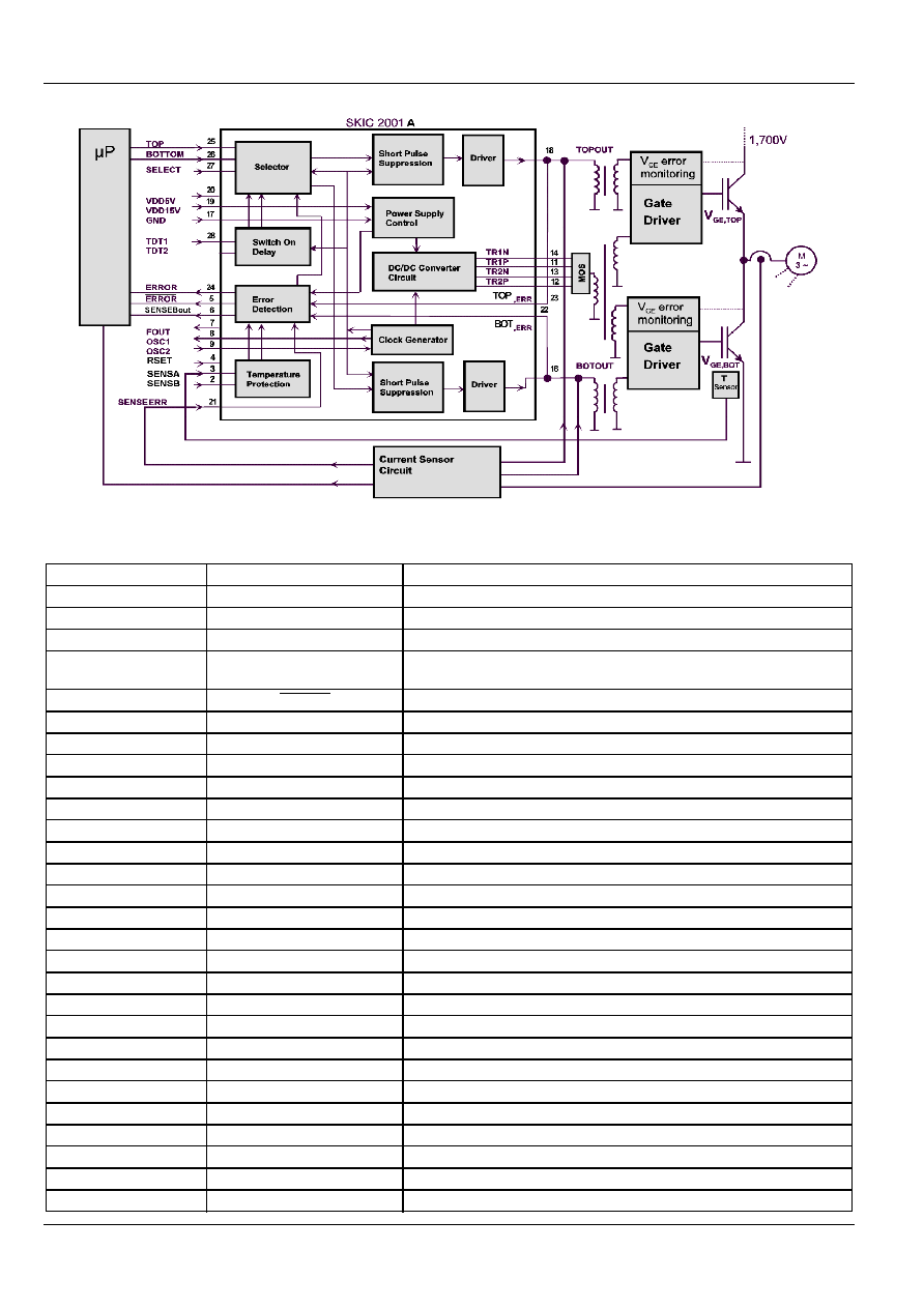
Fig. 1
Functional block diagram of the Control IC (SKIC2001A) inside a propulsion control

© by SEMIKRON
0699
3
I
:
\
M
AR
KETIN\
F
RA
MED
AT\
datbl\
Treiber\Sk
i
c
2001AB
.
fm
Overview
The integrated intelligent controller circuit (SKIC 2001)
presented for the control of IGBTs, especially in a
halfbridge, for high power applications (up to 1,700 V
and several hundred amperes) and frequencies up to
50
kHz. It includes several driver, protection and
monitor functions. Fig. 1. shows the functional block
diagram of the control IC inside a propulsion control. It
consists of a digital control unit, mostly a microprocessor
(µP), the control IC (SKIC 2001), a potential separation
(ferrite signal transformer or opto-couplers), the gate
driver stages, an IGBT halfbridge and a consumer, in
this case a motor.
With aid of the digital unit a pulse frequency modulation
of the IGBT driver signals is possible and, therefore, a
power control of the consumer can be realized. The
developed control circuit contains the signal processing,
power supply, the driving and monitoring functions for
two IGBTs in a halfbridge (application also for SIXPACK
and single switch possible). A power supply of 5 V and
15 V (12 V for SKIC
2001 B) is necessary.
The most important parts, functions, connections and in-
and outputs are shown in Fig. 1:
∑
the forward branch with selector, switch on delay, short
pulse suppression, driver and signal transformer to the
secondary side (high voltage side)
∑
the backward branch with error detection and process-
ing (undervoltage, temperature, V
CE
and overcurrent)
∑
the additional part with clock generator, power supply
control and dc/dc converter circuit
The control circuit has several inputs, some of them with
a Schmitt-trigger characteristic for increased noise
immunity. TOP and BOTTOM are the main control
inputs. RESET sets back the error storage. With TDT1,
TDT2 and SELECT a switch on delay between 0 and
4
µs can be chosen. SENSA, SENSB (temperature
sensor) and RSET are optional inputs, if the customer
applies a temperature monitoring. The KTY85 is used as
temperature sensor which is placed insulated on the
DCB-substrate. Thus the temperature of the heat sink is
determined. With input RSET the variation of the
comparator thresholds (A and B) or adaptations to an
other sensor are possible with the help of an external
resistance. The error signal of comparator A sets the
internal error storage. The error signal of comparator B
lies at output SENSB_OUT.
With the use of ferrite signal transformers the information
between primary and secondary side may flow in both
directions and high levels of dv/dt and insulation are
guaranteed (opto-couplers are also possible). The high
frequency dc/dc converter avoids the requirement of an
externally insulated power supply to obtain the
necessary voltage and power for the IGBT gates. For
this operation the dc/dc converter circuit supplies a
15
V signal with a frequency of 500
kHz. There is the
possibility to use one halfbridge of external power
MOSFET (1 pMOS and 1 nMOS) for a lower power
supply or a bridge (2 pMOS and 2 nMOS) for a higher
power supply.
The IGBT driver stages are externally placed. So the
stages can be matched to the respective power range
and the optimum function (switching frequency and gate
charge of the IGBTs, negative switch off voltage, soft
turn off). A short circuit at the IGBT driver stages can be
monitored by a permanent control of the collector-
emitter-voltage (optionally). In general this method is
used, but it has the disadvantage, that a time of a few µs
has to be waited, until it can be decided between a
normal switch on or a short circuit by the V
CE
-value. A
better and faster method is the evaluation of a differential
quotient of the V
CE
-drop. In the case of a detected short
circuit, the IGBT is switched off immediately and an error
signal V
CE
-error is transformed to the control IC.
Another (optional) way to detect a short circuit is the use
of a current sensor at the output of the halfbridge (Fig. 1).
For high power application a current measuring signal is
fundamentally indispensable for an optimum
microprocessor control of the propulsion system. We
use a newly developed compensating current sensor on
the basis of a magnetic field sensor. It can be placed
outside or inside the power module. The sensor current
(in a ratio of 2000 : 1 to the output current) is converted
into a proportional analog voltage signal in the separate
sensor circuit and evaluated by the microprocessor. In
addition the sensor circuit contains a comparator stage
where the same signal is also used for the overcurrent
monitoring of the IGBTs. In case of an overcurrent the
IGBTs are switched off directly in about 1 µs and then an
error signal I
ERR
is sent to the control IC. The advantage
of this solution is the saving of the expensive V
CE
-
monitoring and the very short reaction time to a short
circuit.
An internal protection function of the SKIC 2001 is the
power supply control. The circuit will be blocked, if the
15V-power supply (12 V for SKIC 2001 B) drops under a
value of about 13,0 V (about 10 V for SKIC 2001 B). In
this case a safe function, especially of the transformers,
can't be guaranteed any longer.
All detected error signals are processed in the control IC.
The forward driver signal is blocked or the IGBTs are
switched off and error signals are given at the output to
the microprocessor (ERROR and ERROR for
undervoltage of power supply, V
CE
-error and over
temperature). The error storage can be reset by a
RESET pulse, which is generated, if 9
µ
s the inputs
(TOP, BOTTOM) are LOW.
4
0699
© by SEMIKRON
Functional description
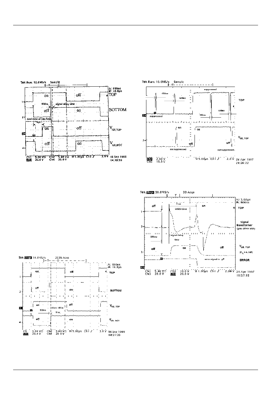
Interlock
Fig. 2 demonstrate the right function of interlock of TOP-
and BOTTOM-IGBT.
Fig. 2
Interlock function
At first BOTTOM is switched off immediately after the
corresponding input signal (at 5 µs), while TOP is switched
on with a delay of about 1 µs (setting of interlock 4 µs).
After 10 µs both inputs become ,,on". This isn't a correct
state (both IGBT ,,on" means short circuit) and that is why
both are switched off. A switch on of BOTTOM is possible
not before TOP is ,,off" (at 25 µs, interlock and delay time
about 5 µs).
Fig. 3 shows the behavior, if the interlock function isn't
active (SELECT ,,low"). Both outputs react immediately to
the corresponding input (the difference is the signal delay
time).
Fig. 3
Interlock function not active
Shortpulse suppression
Fig. 4 presents the short pulse suppression. Pulses
shorter than 480 ns are suppressed (noise) and pulse
longer than 640 ns are valid.
Fig. 4 Short pulse suppression
V
CEsat
error processing
Fig. 5 V
CE
-error processing
In Fig. 5 the signals at the signal transformer are
described. About 860 ns after TOP is ,,on" (delay time), we
see a positive needle on the transformer at the gate driver
side and the IGBT will switch on. After about 3 µs a V
CE
-
error signal will appear, the IGBT will switch off and an
error-signal (smaller positive needle) is transformed to the
low voltage side. The control IC processes this signal and
gives an off impulse (negative needle) to the IGBT. (The
needles on the transformers are converted in rectangular
pulses by a gate driver input with Schmitt trigger-
characteristic).
© by SEMIKRON
0699
5
I
:
\
M
AR
KETIN\
F
RA
MED
AT\
datbl\
Treiber\Sk
i
c
2001AB
.
fm
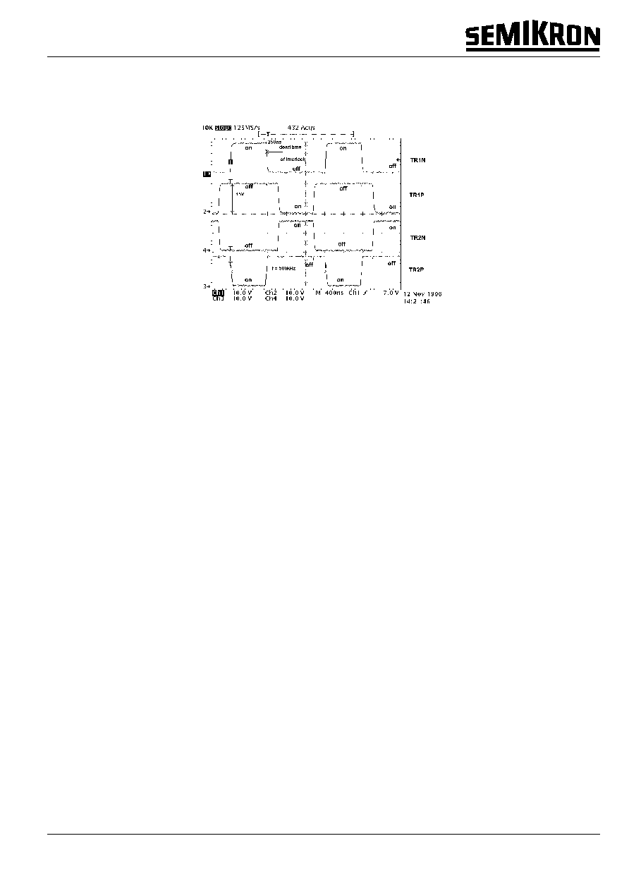
DC-DC-Converter-Control signals
Fig. 6
DC/DC converter signals
Fig. 6 presents the output driver signals of dc/dc converter. The interlock time is 250 ns, the frequency is 500 kHz.