© by SEMIKRON
010315
B 18 ≠ 41
SKiM 350 GD 128 DM
Absolute Maximum Ratings
Values
Symbol Conditions
1)
Units
V
CES
V
CGR
I
C
I
CM
V
GES
P
tot
T
j
, (T
stg
)
T
cop
V
isol
humidity
climate
R
GE
= 20 k
T
HS
= 25/70 ∞C
T
HS
= 25/70 ∞C; t
p
= 1 ms
per IGBT, T
HS
= 25 ∞C
max. case operating temperature
AC, 1 min.
IEC-EN 60721-3-3
IEC 68 T.1
1200
1200
300 / 230
600 / 460
± 20
925
≠ 40 ... +150 (125)
125
2500
40/125/56
V
V
A
A
V
W
∞C
∞C
V
Inverse Diode
I
F
= ≠I
C
I
FM
= ≠I
CM
I
FSM
I
2
t
T
HS
= 25/70 ∞C
T
HS
= 25/70 ∞C; t
p
= 1 ms
t
p
= 10 ms; sin.; T
j
= 150 ∞C
t
p
= 10 ms; T
j
= 150 ∞C
300 / 230
600 / 460
2200
24 200
A
A
A
A
2
s
Characteristics
Symbol Conditions
1)
min.
typ.
max. Units
V
(BR)CES
V
GE(th)
I
CES
I
GES
V
CEsat
4)
V
GE
= 0, I
C
= 1 mA
V
GE
= V
CE
, I
C
= 4 mA
V
GE
= 0
V
CE
= V
CES
T
j
= 125 ∞C
V
GE
= 20 V, V
CE
= 0
I
C
= 200 A
V
GE
= 15 V;
T
j
= 25 ∞C
V
CES
4,5
≠
≠
≠
≠
5,5
15
≠
2,0
≠
6,5
≠
500
2,3
V
V
mA
nA
V
C
ies
C
oes
C
res
L
CE
R
CC¥+ EE¥
V
GE
= 0
V
CE
= 25 V
f = 1 MHz
resistance, terminal-chip; T
HS
= 25 ∞C
≠
≠
≠
≠
≠
18
4,3
3,6
≠
1,35
≠
20
≠
nF
nF
nF
nH
m
t
d(on)
t
r
t
d(off)
t
f
E
on
E
off
V
CC
= 600 V
V
GE
= +15 V / ≠15 V
3)
I
C
= 200 A, ind. load
R
Gon
= R
Goff
= 5
T
j
= 125 ∞C
≠
≠
≠
≠
≠
≠
150
45
700
50
21
20
≠
≠
≠
≠
≠
≠
ns
ns
ns
ns
mJ
mJ
Inverse Diode
8)
V
F
= V
EC
V
F
= V
EC
V
TO
r
T
I
RRM
Q
rr
I
F
= 200 A
V
GE
= 0 V;
I
F
= 100 A
T
j
= 25 (125) ∞C
T
j
= 125 ∞C
T
j
= 125 ∞C
I
F
= 200 A; T
j
= 25 (125) ∞C
2)
I
F
= 200 A; T
j
= 25 (125) ∞C
2)
≠
≠
≠
≠
≠
≠
2,3 (2,1)
1,8 (1,6)
1,1
5
TBD
TBD
2,6
≠
≠
V
V
V
m
A
µC
Thermal Characteristics
5)
R
thjh
R
thjhD
R'
thjc
6)
R'
thjcD
6)
per IGBT
per diode
per IGBT
per diode
≠
≠
≠
≠
≠
≠
≠
≠
0,135
0,185
0,031
0,046
∞C/W
∞C/W
∞C/W
∞C/W
Temperature Sensor
R
TS
tolerance
T = 25 ∞C / 100 ∞C
T = 25 ∞C / 100 ∞C
≠
≠
1,0 / 1,67
3,0 / 2,0
≠
≠
k
%
SKiM
Æ
4
IGBT Modules
SKiM 350 GD 128 DM
Preliminary Data
Features
∑
N channel, homogeneous planar
IGBT Silicon structure with n+
buffer layer in SPT (soft punch
through) technology
∑
Low inductance case
∑
Fast & soft inverse CAL diodes
8)
∑
Isolated by AlN DCB (Direct
Copper Bonded) ceramic plate
∑
Pressure contact technology for
thermal contacts
∑
Spring contact system to attach
driver PCB to the control
terminals
∑
Integrated temperature sensor
Typical Applications
∑
Switched mode power supplies
∑
Three phase inverters for AC
motor speed control
∑
Switching (not for linear use)
1)
T
HS
= 25 ∞C, unless otherwise
specified
2)
TBD
3)
Use V
GEoff
= ≠ 5 ... ≠ 15 V
4)
Measured at chip level
5)
See mounting instructions
6)
Corresponding value. This value
cannot be measured. It is only given
for comparison.
8)
CAL = Controlled Axial Lifetime
Technology
GD
B 18 ≠ 42
020315
© by SEMIKRON
SKiM 350 GD 128 DM
0
10
20
30
40
50
60
0
100
200
300
400
500
I
C
A
E
mJ
E
on
E
off
SKiM 350GD128DM.xls - 1
0
10
20
30
40
50
60
0
5
10
15
20
25
R
G
E
mJ
E
on
E
off
SKiM 350GD128DM.xls - 2
0,1
1
10
100
1000
1
10
100
1000
10000
V
CE
V
I
C
A
t
p
=16µs
100µs
1ms
10ms
SKiM 350GD128DM.xls - 3
0
0,5
1
1,5
2
2,5
0
200
400
600
800
1000 1200 1400
V
CE
V
I
Cpuls
/I
C
SKiM 350GD128DM.xls - 4
0
2
4
6
8
10
0
200
400
600
800
1000 1200 1400
V
CE
V
I
CSC
/I
C
allowed numbers of
short circuits: <1000
time between short
circuits: >1s
SKiM 350GD128DM.xls - 5
0
50
100
150
200
250
300
350
0
20
40
60
80
100 120 140 160
Ths
∞C
I
C
A
SKiM 350GD128DM.xls - 6
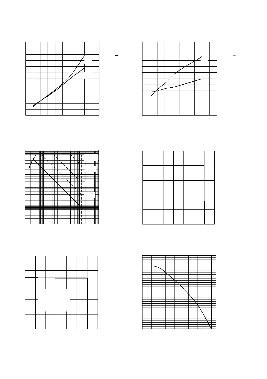
Fig. 1
Turn-on /-off energy = f (I
C
)
Fig. 2 Turn-on /-off energy = f (R
G
)
T
j
= 125 ∞C
V
CE
= 600 V
V
GE
= + 15 V
R
G
= 5
1 pulse
T
HS
= 25 ∞C
T
j
150 ∞C
T
j
=
125 ∞C
V
GE
= ± 15 V
t
sc
=
10 µs
L < 25 nH
V
CC
= 900 V
I
CN
= 200 A
T
j
=
125 ∞C
V
GE
= ± 15 V
R
Goff
= 5
V
CC
= 1000 V
I
C
= 200 A
Fig. 5 Safe operating area at short circuit I
C
= f (V
CE
)
Fig. 6 Rated current vs. temperature I
C
= f (T
HS
)
Fig. 3 Maximum safe operating area (SOA) I
C
= f (V
CE
)
Fig. 4 Turn-off safe operating area (RBSOA)
T
j
= 150 ∞C
V
GE
15 V
T
j
= 125 ∞C
V
CE
= 600 V
V
GE
= + 15 V
I
C
= 200 A
© by SEMIKRON
010315
B 18 ≠ 43
SKiM 350 GD 128 DM
0
50
100
150
200
250
300
350
400
0
1
2
3
4
V
CE
V
I
C
A
17V
15V
13V
11V
9V
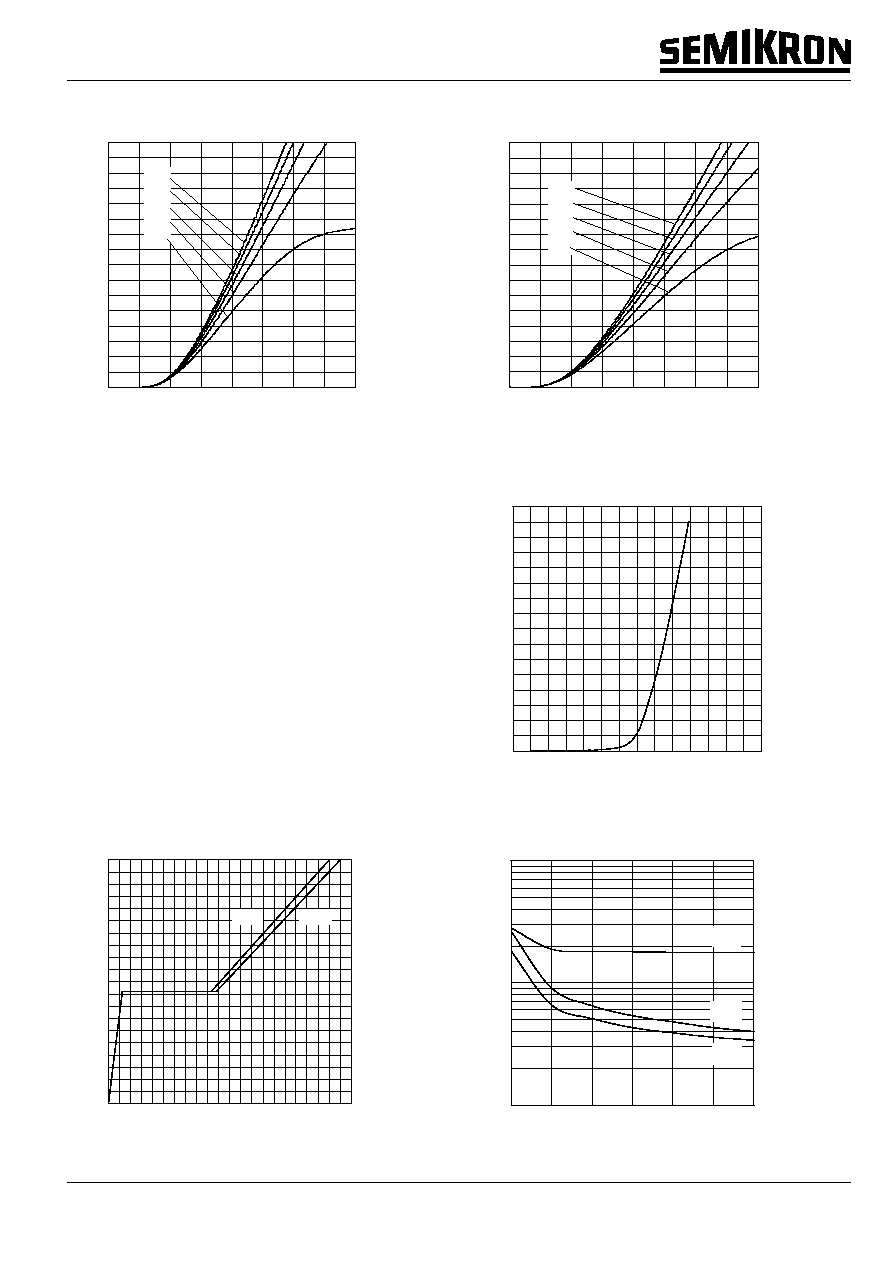
SKiM 350GD128DM.xls - 7
0
50
100
150
200
250
300
350
400
0
1
2
3
4
V
CE
V
I
C
A
17V
15V
13V
11V
9V
SKiM 350GD128DM.xls - 8
0
50
100
150
200
250
300
350
400
0
2
4
6
8
10
12
14
V
G
V
I
C
A
SKiM 350GD128DM.xls - 10
0
2
4
6
8
10
12
14
16
18
20
0
500
1000
1500
2000
Q
Gate
nC
V
GE
V
600
800V
SKiM 350GD128DM.xls - 11
1
10
100
0
5
10
15
20
25
30
V
CE
V
C
nF
C
ies
C
oes
C
res
SKiM 350GD128DM.xls - 12
Fig. 9 Saturation characteristic (IGBT)
Calculation elements and equations
Fig. 10 Typ. transfer characteristic, t
p
= 80 µs; V
CE
= 20 V
Fig. 7
Typ. output characteristic, t
p
= 80 µs; 25 ∞C
Fig. 8 Typ. output characteristic, t
p
= 80 µs; 125 ∞C
Fig. 11 Typ. gate charge characteristic
Fig. 12 Typ. capacitances vs. V
CE
V
GE
= 0 V
f = 1 MHz
I
Cpuls
= 200 A
B 18 ≠ 44
020315
© by SEMIKRON
SKiM 350 GD 128 DM
10
100
1000
0
100
200
300
400
500
I
C
A
t
ns
t
doff
t
don
t
r
t
f
SKiM 350GD128DM.xls - 13
10
100
1000
10000
0
5
10
15
20
25
R
G
t
ns
t
doff
t
don
t
r
t
f
SKiM 350GD128DM.xls - 14
0
100
200
300
400
0
1
2
3
4
V
F
V
I
F
A
T
j
=125∞C, typ.
T
j
=25∞C, typ.
SKiM 350GD128DM.xls - 15
0,00001
0,0001
0,001
0,01
0,1
1
0,00001 0,0001
0,001
0,01
0,1
1
10
t
p
s
Z
thJHS
K/W
D=0,50
0,20
0,10
0,05
0,02
0,01
single pulse
SKiM 350GD128DM.xls - 17
0,0001
0,001
0,01
0,1
1
0,00001 0,0001
0,001
0,01
0,1
1
10
s
Z
thJHS
K/W
D=0,5
0,2
0,1
0,05
0,02
0,01
single pulse
t
p
SKiM 350GD128DM.xls - 180
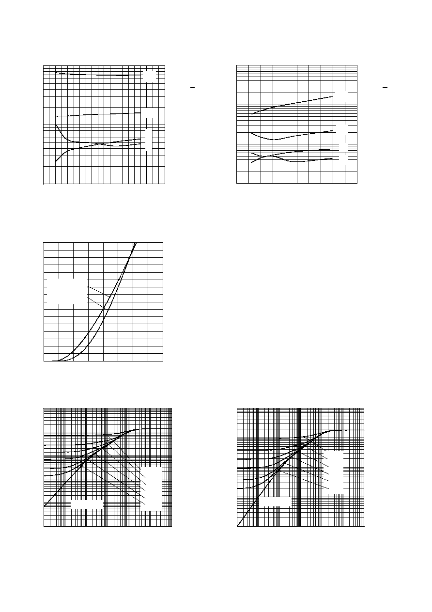
Fig. 15 Typ. CAL diode forward characteristic
Fig. 16 Diode turn-off energy dissipation per pulse
Fig. 13 Typ. switch times vs. I
C
Fig. 14 Typ. switch times vs. gate resistor R
G
Fig. 17 Transient thermal impedance of IGBT
Z
thJHS
= f (t
p
); D = t
p
/ t
c
= t
p
∑ f
Fig. 18 Transient thermal impedance of
inverse CAL diodes Z
thJHS
= f (t
p
); D = t
p
/ t
c
= t
p
∑ f
T
j
= 125 ∞C
V
CE
= 600 V
V
GE
= + 15 V
I
C
= 200 A
ind. load
T
j
= 125 ∞C
V
CE
= 600 V
V
GE
= + 15 V
R
Gon
= R
Goff
=
5
ind. load
© by SEMIKRON
010315
B 18 ≠ 45
SKiM 350 GD 128 DM
This is an electrostatic discharge sensitive device (ESDS).
Please observe the international standard IEC 747-1, Chapter IX.
Mechanical Data
Symbol Conditions
Values
Units
min.
typ.
max.
M
1
M
2
a
w
to heatsink, SI Units
(M5)
to heatsink, US Units
for terminals, SI Units
(M6)
for terminals, US Units
2
18
4
35
≠
≠
≠
≠
≠
≠
≠
≠
3
26
5
44
5x9,81
310
Nm
lb.in.
Nm
lb.in.
m/s
2
g
SKiM 4
SKiM 350 GD 128 DM
This technical information specifies semiconductor devices but promises no characteristics. No warranty or guarantee expressed or
implied is made regarding delivery, performance or suitability.
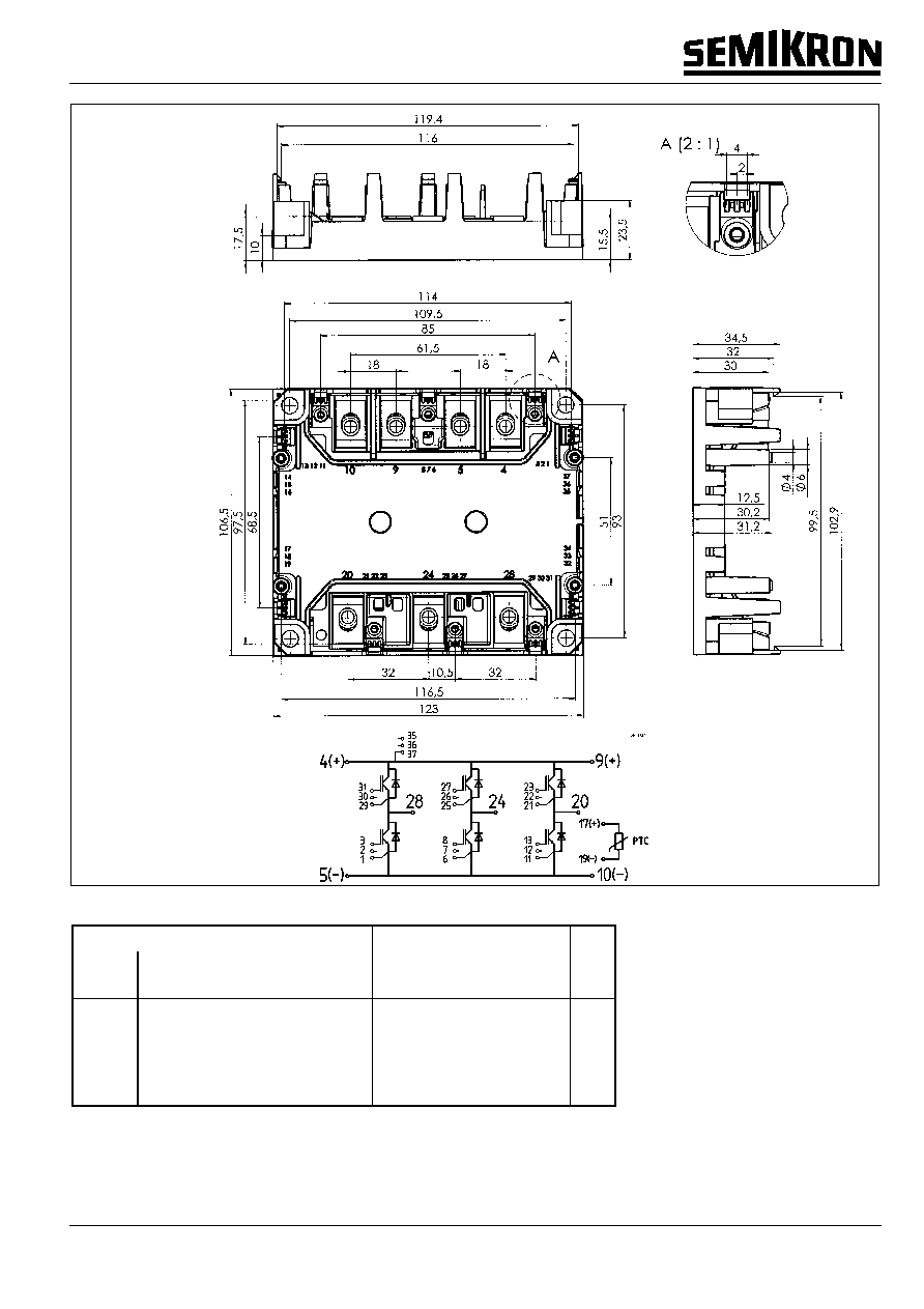
Dimensions in mm
Case outline and circuit diagram

B 18 ≠ 46
020315
© by SEMIKRON
SKiM 350 GD 128 DM