 | –≠–ª–µ–∫—Ç—Ä–æ–Ω–Ω—ã–π –∫–æ–º–ø–æ–Ω–µ–Ω—Ç: SFS4416 | –°–∫–∞—á–∞—Ç—å:  PDF PDF  ZIP ZIP |

Absolute Maximum Ratings
Symbol
Parameter
Value
Units
V
DSS
Drain to Source Voltage
30
V
I
D
Continuous Drain Current(@T
A
= 25
∞C)
9
A
I
DM
Drain Current Pulsed
(Note 1)
50
A
V
GS
Gate to Source Voltage
±
20
V
P
D
Total Power Dissipation Single Operation (T
A
=25
∞C
)
2.5
W
Total Power Dissipation Single Operation (T
A
=70
∞C
)
1.6
W
T
STG,
T
J
Operating Junction Temperature & Storage Temperature
- 55 ~ 150
∞C
T
L
Maximum Lead Temperature for soldering purpose,
1/8 from Case for 10 seconds.
300
∞C
Thermal Characteristics
Symbol
Parameter
Value
Units
Min.
Typ.
Max.
R
JA
Thermal Resistance, Junction-to-Ambient
(Note 4)
-
-
50
∞C/W
SFS4416
January, 2003. Rev. 0.
1/6
Features
Low R
DS(on)
(Max 0.018 )@V
GS
=10V
Low R
DS(on)
(Max 0.028 )@V
GS
=4.5V
Gate Charge (Typical 16nC)
Maximum Junction Temperature Range (150∞C)
Available in Tape and Reel
General Description
This Power MOSFET is produced using Semiwell's advanced
planar stripe, DMOS technology. This latest technology has been
especially designed to minimize on-state resistance, have a low
gate charge with superior switching performance, and rugged
avalanche characteristics. This Power MOSFET is well suited
for power management circuit or DC-DC converter.
SemiWell
Semiconductor
Copyright@SemiWell Semiconductor Co., Ltd., All rights reserved.
Logic N-Channel MOSFET
8-SOIC
Symbol
S
G
D
1
2
3
4
5
6
7
8
D
D
D
S
S
D
D
D
D
S
S
G
S

SFS4416
Electrical Characteristics
( T
J
= 25 ∞C unless otherwise noted )
Symbol
Parameter
Test Conditions
Min
Typ
Max
Units
Off Characteristics
BV
DSS
Drain-Source Breakdown Voltage
V
GS
= 0V, I
D
= 250uA
30
-
-
V
BV
DSS
/
T
J
Breakdown Voltage Temperature
coefficient
I
D
= 250uA, referenced to 25 ∞C
-
15
-
mV/∞C
I
DSS
Drain-Source Leakage Current
V
DS
= 24V, V
GS
= 0V
V
DS
= 24V, V
GS
= 0V, T
J
= 55 ∞C
-
-
1
25
uA
I
GSS
Gate-Source Leakage, Forward
V
GS
= 20V, V
DS
= 0V
100
nA
Gate-Source Leakage, Reverse
V
GS
= -20V, V
DS
= 0V
-
-
-100
nA
On Characteristics
V
GS(th)
Gate Threshold Voltage
V
DS
= V
GS
, I
D
= 250uA
1.0
-
-
V
R
DS(ON)
Static Drain-Source On-state
Resistance
V
GS
= 10 V, I
D
= 9A
V
GS
= 4.5 V, I
D
= 7.3A
-
-
0.013
0.018
0.018
0.028
Dynamic Characteristics
C
iss
Input Capacitance
V
GS
=0 V, V
DS
=15V, f = 1MHz
-
920
-
pF
C
oss
Output Capacitance
-
490
-
C
rss
Reverse Transfer Capacitance
-
150
-
Dynamic Characteristics
t
d(on)
Turn-on Delay Time
V
DD
= 15V, I
D
= 1A, R
G
= 50
V
GS
= 10 V
(Note 2,3)
-
13
20
ns
t
r
Rise Time
-
23
50
t
d(off)
Turn-off Delay Time
-
130
150
t
f
Fall Time
-
65
100
Q
g
Total Gate Charge
V
DS
= 15V, V
GS
= 5V, I
D
= 9A
(Note 2,3)
-
16
20
nC
Q
gs
Gate-Source Charge
-
4
-
Q
gd
Gate-Drain Charge(Miller Charge)
-
7.5
-
Source-Drain Diode Ratings and Characteristics
Symbol
Parameter
Test Conditions
Min.
Typ.
Max.
Unit.
I
S
Continuous Source Diode Forward Current
-
-
2.1
A
V
SD
Diode Forward Voltage
I
S
= 2.1A, V
GS
=0V
(Note 2)
-
-
1.2
V
NOTES
1. Repeativity rating : pulse width limited by junction temperature
2. Pulse Test : Pulse Width 300us, Duty Cycle 2%
3. Essentially independent of operating temperature.
4. Surface mounted on 1 inch
2
Cu board.
2/6
0
5
10
15
20
25
30
35
40
45
50
0
10
20
30
40
50
V
GS
= 10V
V
GS
= 4.5V
Note : T
J
= 25
R
DS
(
O
N
)
,
Drai
n-S
o
urce
On
-Re
s
i
s
t
a
n
c
e
[
m
]
I
D
, Drain Current [A]
0.0
0.2
0.4
0.6
0.8
1.0
1.2
1.4
10
0
10
1
150
Notes :
1. V
GS
= 0V
2. 250µ s Pulse Test
25
I
DR
,
Re
vers
e Dr
ain Cu
rr
ent
[
A
]
V
SD
, Source-Drain voltage [V]
0
1
2
3
4
5
10
0
10
1
150
o
C
25
o
C
-55
o
C
Notes :
1. V
DS
= 15V
2. 250µ s Pulse Test
I
D
,
D
r
a
i
n
C
u
r
r
en
t [A]
V
GS
, Gate-Source Voltage [V]
10
-1
10
0
10
1
V
GS
Top : 10.0 V
8.0 V
6.0 V
5.0 V
4.5 V
4.0 V
3.5 V
Bottom : 3.0 V
Notes :
1. 250µ s Pulse Test
2. T
C
= 25
I
D
,
D
r
ain Curr
ent
[
A
]
V
DS
, Drain-Source Voltage [V]
0
5
10
15
20
25
30
35
0
2
4
6
8
10
12
V
DS
= 15V
V
DS
= 24V
Note : I
D
= 1 A
V
GS
,
G
a
t
e
-
S
o
u
r
c
e Volt
ag
e [
V
]
Q
G
, Total Gate Charge [nC]
0
5
10
15
20
25
30
0
500
1000
1500
2000
2500
C
rss
C
oss
C
iss
Notes :
1. V
GS
= 0V
2. f=1MHz
C
iss
=C
gs
+C
gd
(C
ds
=shorted)
C
oss
=C
ds
+C
gd
C
rss
=C
gd
C
a
p
a
citan
c
e [pF
]
V
DS
, Drain-Source Voltage [V]
3/6
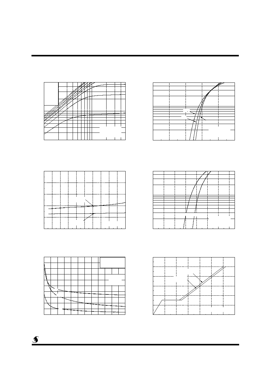
Fig 3. On Resistance Variation vs.
Drain Current and Gate Voltage
Fig 4. On State Current vs.
Allowable Case Temperature
Fig 5. Capacitance Characteristics
Fig 6. Gate Charge Characteristics
SFS4416
Fig 1. On-State Characteristics
Fig 2. Transfer Characteristics

-100
-50
0
50
100
150
200
0.0
0.5
1.0
1.5
2.0
Notes :
1. V
GS
= 10 V
2. I
D
= 9 A
R
DS
(
O
N)
,
(
N
or
ma
lized)
D
r
ai
n
-
S
o
urce O
n
-
R
e
s
i
s
t
a
nce
T
J
, Junction Temperature [
o
C]
-100
-50
0
50
100
150
200
0.8
0.9
1.0
1.1
1.2
Notes :
1. V
GS
= 0 V
2. I
D
= 250 µ A
BV
DSS
,
(
N
or
m
a
liz
ed)
Dr
ain-
Sour
ce
B
r
e
a
k
d
ow
n Volt
a
g
e
T
J
, Junction Temperature [
o
C]
1 0
-4
1 0
-3
1 0
-2
1 0
-1
1 0
0
1 0
1
1 0
2
1 0
-3
1 0
-2
1 0
-1
1 0
0
N o te s :
1 . Z
J C
(t) = 1 .0
/W M a x .
2 . D u ty F a c to r, D = t
1
/t
2
3 . T
J M
- T
C
= P
D M
* Z
J C
(t)
s in g le p u ls e
D = 0 .5
0 .0 2
0 .2
0 .0 5
0 .1
0 .0 1
Z
JC
(t), Ther
ma
l Re
sp
on
s
e
t
1
, S q u a re W a v e P u ls e D u ra tio n [s e c ]
Fig 9. Normalized Transient Thermal Response Curve
Fig 7. Breakdown Voltage Variation
vs. Junction Temperature
Fig 8. On-Resistance Variation
vs. Junction Temperature
SFS4416
4/6

5/6
Fig 11. Switching Time Test Circuit & Waveforms
SFS4416
Fig. 10. Gate Charge Test Circuit & Waveforms
V
in
V
DS
10%
90%
t
d(on)
t
r
t
on
t
off
t
d(off)
t
f
10V
V
DS
R
L
DUT
Pulse
Generator
V
in
V
DS
10%
90%
t
d(on)
t
r
t
on
t
off
t
d(off)
t
f
V
in
V
DS
10%
90%
t
d(on)
t
r
t
on
t
off
t
d(off)
t
f
V
DD
V
DD
V
V
DS
R
L
DUT
Pulse
Generator
R
G
V
in
V
in
V
DS
10%
90%
t
d(on)
t
r
t
on
t
off
t
d(off)
t
f
V
in
V
DS
10%
90%
t
d(on)
t
r
t
on
t
off
t
d(off)
t
f
10V
V
DS
R
L
DUT
Pulse
Generator
V
in
V
DS
10%
90%
t
d(on)
t
r
t
on
t
off
t
d(off)
t
f
V
in
V
DS
10%
90%
t
d(on)
t
r
t
on
t
off
t
d(off)
t
f
V
DD
V
DD
V
DD
V
DD
V
V
DS
R
L
DUT
Pulse
Generator
R
G
V
in
Charge
V
GS
5 V
Q
g
Q
gs
Q
gd
1mA
V
GS
DUT
V
DS
300nF
50K
200nF
12V
Same Type
as DUT
Charge
V
GS
V
Q
g
Q
gs
Q
gd
Charge
V
GS
V
Q
g
Q
gs
Q
gd
1mA
V
GS
DUT
V
DS
300nF
50K
200nF
12V
Same Type
as DUT
Charge
V
GS
5 V
Q
g
Q
gs
Q
gd
Charge
V
GS
5 V
Q
g
Q
gs
Q
gd
1mA
V
GS
DUT
V
DS
300nF
50K
200nF
12V
Same Type
as DUT
Charge
V
GS
V
Q
g
Q
gs
Q
gd
Charge
V
GS
V
Q
g
Q
gs
Q
gd
1mA
V
GS
DUT
V
DS
300nF
50K
200nF
12V
Same Type
as DUT

Dim.
mm
Inch
Min.
Typ.
Max.
Min.
Typ.
Max.
A
1.35
1.55
1.75
0.053
0.061
0.069
B
0.1
0.175
0.25
0.004
0.007
0.010
C
0.38
0.445
0.510
0.015
0.018
0.020
D
0.19
0.22
0.25
0.007
0.009
0.010
E
4.8
4.9
5
0.189
0.193
0.197
F
3.8
3.9
4
0.150
0.154
0.157
G
1.27 BSC
H
5.8
6
6.2
0.228
0.236
0.244
I
0.5
0.715
0.93
0.020
0.028
0.037
J
0'
4'
8'
0'
4'
8'
K
0.250
0.375
0.05
0.010
0.015
0.020
SFS4416
8-SOIC Package Dimension
6/6
A
B
0.1
E
G
C
D
J
H
I
K
45
∞
◊
0.254(
Ga
p plane)
F