Absolute Maximum Ratings
( T
J
= 25∞C unless otherwise specified )
Symbol
Parameter
Condition
Ratings
Units
V
DRM
Repetitive Peak Off-State Voltage
Sine wave, 50 to 60 Hz, Gate open
600
V
I
T(RMS)
R.M.S On-State Current
T
C
= 99 ∞C, Full Sine wave
4.0
A
I
TSM
Surge On-State Current
One Cycle, 50Hz/60Hz, Peak,
Non-Repetitive
30/33
A
I
2
t
I
2
t
for Fusing
tp = 10ms
4.5
A
2
s
P
GM
Peak Gate Power Dissipation
T
C
= 99 ∞C, Pulse width
1.0
us
3
W
P
G(AV)
Average Gate Power Dissipation
Over any 20ms period
0.3
W
I
GM
Peak Gate Current
tp = 20us, T
J
=125∞C
1.0
A
V
GM
Peak Gate Voltage
tp = 20us, T
J
=125∞C
7.0
V
T
J
Operating Junction Temperature
- 40 ~ 125
∞C
T
STG
Storage Temperature
- 40 ~ 150
∞C
Mass
2.0
g
Features
Repetitive Peak Off-State Voltage : 600V
R.M.S On-State Current ( I
T(RMS)
= 4 A )
High Commutation dv/dt
Sensitive Gate Triggering 4 Mode
General Description
This device is sensitive gate triac suitable for direct coupling
to TTL, HTL, CMOS and application such as various logic
functions, low power AC switching applications, such as fan
speed, small light controllers and home appliance equipment.
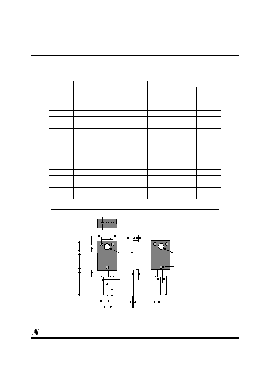
2.T2
3.Gate
1.T1
Symbol
1/6
STF4A60S
SemiWell
Semiconductor
TO-220F
1
2
3
Aug, 2004. Rev.1
copyright@SemiWell Semiconductor Co., Ltd., All rights reserved.
Sensitive Gate Triacs

Electrical Characteristics
Symbol
Items
Conditions
Ratings
Unit
Min.
Typ.
Max.
I
DRM
Repetitive Peak Off-State
Current
V
D
= V
DRM
, Single Phase, Half Wave
T
J
= 125 ∞C
1.0
mA
V
TM
Peak On-State Voltage
I
T
= 6 A, Inst. Measurement
1.6
V
I
+
GT1
Gate Trigger Current
V
D
= 6 V, R
L
=10
5
mA
I
-
GT1
5
I
-
GT3
5
I
+
GT3
8
12
V
+
GT1
Gate Trigger Voltage
V
D
= 6 V, R
L
=10
1.4
V
V
-
GT1
1.4
V
-
GT3
1.4
V
+
GT3
1.6
2.0
V
GD
Non-Trigger Gate Voltage
T
J
= 125 ∞C, V
D
= 1/2 V
DRM
0.2
V
dv/dt
Critical Rate of Rise Off-State
Voltage
T
J
= 125 ∞C, Gate open,
V
D
= V
DRM
67
%
50
V/
(dv/dt)c
Critical Rate of Rise Off-State
Voltage at Commutation
T
J
= 125 ∞C, [di/dt]c = -2.0 A/ms,
V
D
=2/3 V
DRM
5
V/
I
H
Holding Current
5.0
mA
R
th(j-c)
Thermal Impedance
Junction to case
4.0
∞C/W
STF4A60S
2/6
Notes :
1. Pulse Width
300us , Duty cycle
2%
-50
0
50
100
150
10
1
10
2
10
3
V
+
GT3
X 10
0 (
%
)
V
GT
(t
o
C)
V
+
GT1
V
-
GT1
V
-
GT3
V
GT
(25
o
C)
Junction Temperature [
o
C]
0.0
0.5
1.0
1.5
2.0
2.5
3.0
3.5
4.0
4.5
5.0
95
100
105
110
115
120
125
130
= 90
o
= 150
o
= 60
o
= 30
o
= 180
o
= 120
o
A
l
l
o
w
a
bl
e C
a
se
Temp
era
t
u
r
e
[
o
C]
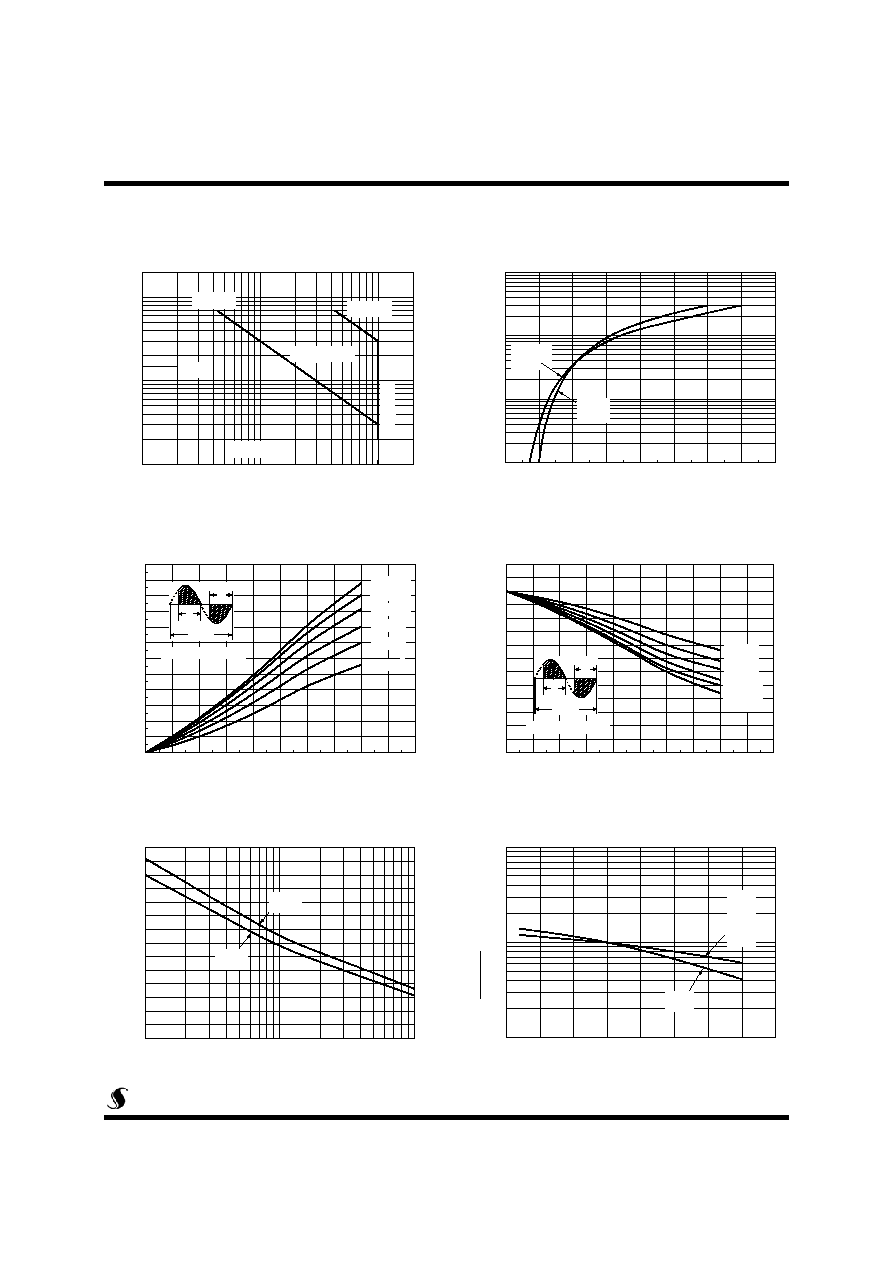
RMS On-State Current [A]
0.0
0.5
1.0
1.5
2.0
2.5
3.0
3.5
4.0
4.5
5.0
0.0
0.5
1.0
1.5
2.0
2.5
3.0
3.5
4.0
4.5
5.0
5.5
6.0
= 90
o
= 150
o
= 60
o
= 30
o
= 180
o
= 120
o
Pow
e
r
Dis
s
ip
at
ion
[
W
]
RMS On-State Current [A]
10
1
10
2
10
3
10
-1
10
0
10
1
V
GD
(0.2V)
25
I
GM
(1
A
)
P
G(AV)
(0.3W)
P
GM
(3W)
V
GM
(7V)
G
a
te
V
o
l
t
a
g
e
[V
]
Gate Current [mA]
10
0
10
1
10
2
0
5
10
15
20
25
30
35
60Hz
50Hz
S
u
r
ge On-S
t
a
te Cu
r
r
en
t
[A
]
Time (cycles)
0.5
1.0
1.5
2.0
2.5
3.0
3.5
4.0
4.5
10
-1
10
0
10
1
10
2
125
o
C
25
o
C
On-State
C
u
r
r
e
n
t
[
A
]
On-State Voltage [V]
STF4A60S
3/6
Fig 1. Gate Characteristics
Fig 2. On-State Voltage
Fig 3. On State Current vs.
Maximum Power Dissipation
Fig 4. On State Current vs.
Allowable Case Temperature
Fig 5. Surge On-State Current Rating
( Non-Repetitive )
Fig 6. Gate Trigger Voltage vs.
Junction Temperature
2
360∞
: Conduction Angle
2
360∞
: Conduction Angle
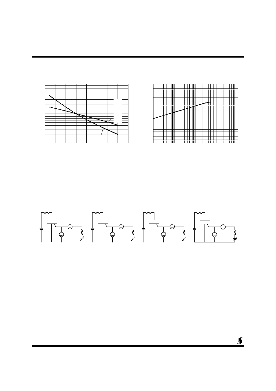
-50
0
50
100
150
10
1
10
2
10
3
I
+
GT3
I
+
GT1
I
-
GT1
I
-
GT3
X
100 (%
)
I
GT
(t
o
C)
I
GT
(25
o
C)
Junction Temperature [
o
C]
10
-2
10
-1
10
0
10
1
10
2
1
10
T
r
ansient T
herm
a
l Im
pedance
[
o
C/
W
]
Time (sec)
4/6
STF4A60S
Fig 8. Transient Thermal Impedance
Fig 7. Gate Trigger Current vs.
Junction Temperature
Fig 9. Gate Trigger Characteristics Test Circuit
A
V
10
6V
R
G
A
V
10
6V
R
G
A
V
10
6V
R
G
Test Procedure
Test Procedure
Test Procedure
A
V
10
6V
R
G
Test Procedure