Absolute Maximum Ratings
( T
J
= 25∞C unless otherwise specified )
Symbol
Parameter
Condition
Ratings
Units
V
DRM
Repetitive Peak Off-State Voltage
600
V
I
T(RMS)
R.M.S On-State Current
T
C
= 94 ∞C
6.0
A
I
TSM
Surge On-State Current
One Cycle, 50Hz/60Hz, Peak,
Non-Repetitive
60/66
A
I
2
t
I
2
t
18
A
2
s
P
GM
Peak Gate Power Dissipation
3.0
W
P
G(AV)
Average Gate Power Dissipation
0.3
W
I
GM
Peak Gate Current
2.0
A
V
GM
Peak Gate Voltage
10
V
V
ISO
Isolation Breakdown Voltage(R.M.S.)
A.C. 1 minute
1500
V
T
J
Operating Junction Temperature
- 40 ~ 125
∞C
T
STG
Storage Temperature
- 40 ~ 150
∞C
Mass
2.0
g
Mar, 2003. Rev. 3
Features
Repetitive Peak Off-State Voltage : 600V
R.M.S On-State Current ( I
T(RMS)
= 6 A )
High Commutation dv/dt
Isolation Voltage ( V
ISO
= 1500V AC )
General Description
This device is fully isolated package suitable for AC switching
application, phase control application such as fan speed and
temperature modulation control, lighting control and static
switching relay.
This device is approved to comply with applicable require-
ments by Underwriters Laboratories Inc.
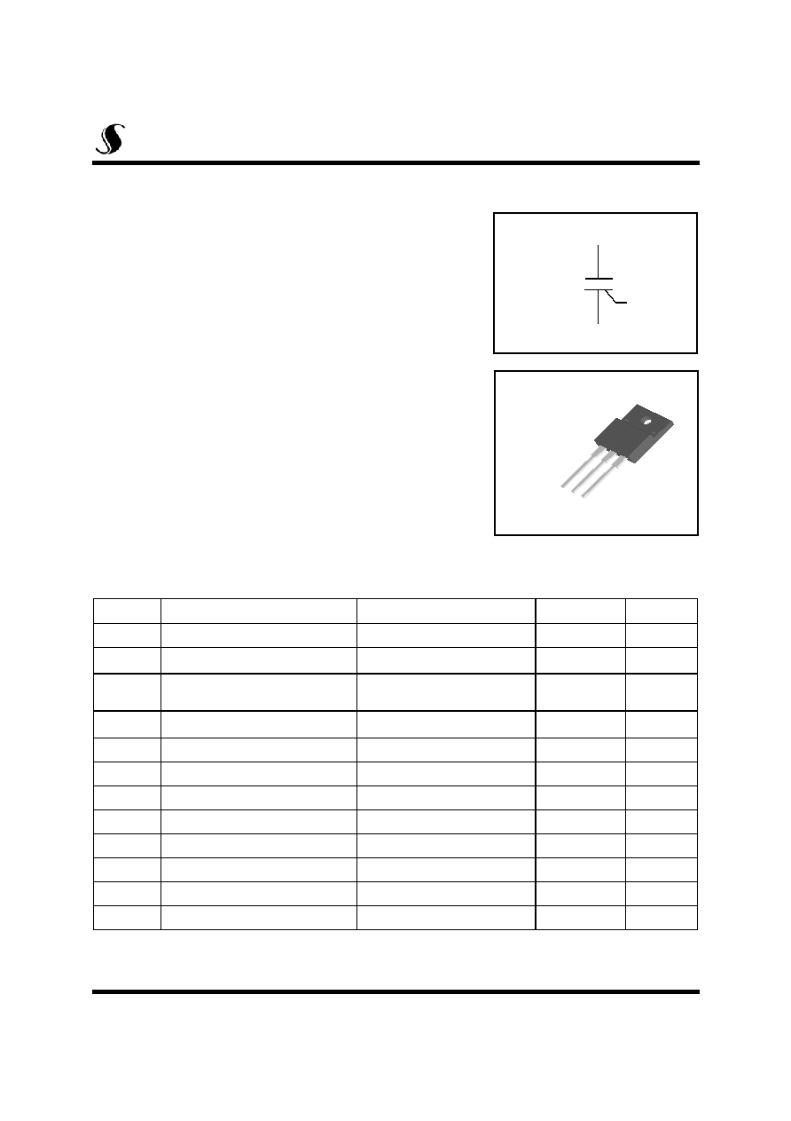
2.T2
3.Gate
1.T1
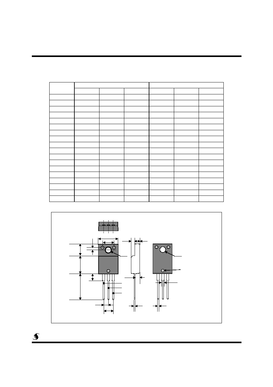
Symbol
TO-220F
1/6
STF6A60
SemiWell
Semiconductor
1
2
3
Bi-Directional Triode Thyristor
copyright@SemiWell Semiconductor Co., Ltd., All rights reserved.
UL : E228720

Electrical Characteristics
Symbol
Items
Conditions
Ratings
Unit
Min.
Typ.
Max.
I
DRM
Repetitive Peak Off-State
Current
V
D
= V
DRM
, Single Phase, Half Wave
T
J
= 125 ∞C
1.0
mA
V
TM
Peak On-State Voltage
I
T
= 8 A, Inst. Measurement
1.5
V
I
+
GT1
Gate Trigger Current
V
D
= 6 V, R
L
=10
20
mA
I
-
GT1
20
I
-
GT3
20
V
+
GT1
Gate Trigger Voltage
V
D
= 6 V, R
L
=10
1.5
V
V
-
GT1
1.5
V
-
GT3
1.5
V
GD
Non-Trigger Gate Voltage
T
J
= 125 ∞C, V
D
= 1/2 V
DRM
0.2
V
(dv/dt)c
Critical Rate of Rise Off-State
Voltage at Commutation
T
J
= 125 ∞C, [di/dt]c = -3.0 A/ms,
V
D
=2/3 V
DRM
5.0
V/
I
H
Holding Current
10
mA
R
th(j-c)
Thermal Impedance
Junction to case
3.8
∞C/W
STF6A60
2/6
0
1
2
3
4
5
6
7
8
90
100
110
120
130
= 90
o
= 150
o
= 60
o
= 30
o
= 180
o
= 120
o
Al
l
o
wabl
e Cas
e
T
e
m
perature [
o
C]
RMS On-State Current [A]
0
1
2
3
4
5
6
7
8
0
1
2
3
4
5
6
7
8
9
10
= 90
o
= 150
o
= 60
o
= 30
o
= 180
o
= 120
o
P
o
w
e
r D
i
s
s
i
pa
tio
n
[W
]
RMS On-State Current [A]
-50
0
50
100
150
0.1
1
10
V
+
GT1
V
_
GT1
V
GT
(t
o
C)
V
_
GT3
V
GT
(25
o
C)
Junction Temperature [
o
C]
0.5
1.0
1.5
2.0
2.5
3.0
3.5
10
0
10
1
10
2
T
J
= 25
o
C
T
J
= 125
o
C
On-State
C
u
r
r
e
n
t
[
A
]
On-State Voltage [V]
10
0
10
1
10
2
0
10
20
30
40
50
60
70
80
60Hz
50Hz
Surg
e O
n
-
S
t
a
t
e
Cur
ren
t
[
A
]
Time (cycles)
10
1
10
2
10
3
10
-1
10
0
10
1
V
GD
(0.2V)
I
GM
(2
A
)
25
P
G(AV)
(0.3W)
P
GM
(3W)
V
GM
(10V)
Ga
t
e
V
o
l
t
age
[V
]
Gate Current [mA]
3/6
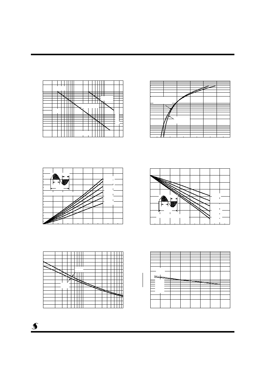
Fig 1. Gate Characteristics
Fig 2. On-State Voltage
Fig 3. On State Current vs.
Maximum Power Dissipation
Fig 4. On State Current vs.
Allowable Case Temperature
Fig 5. Surge On-State Current Rating
( Non-Repetitive )
Fig 6. Gate Trigger Voltage vs.
Junction Temperature
2
360∞
: Conduction Angle
2
360∞
: Conduction Angle
STF6A60
-50
0
50
100
150
0.1
1
10
I
_
GT3
I
+
GT1
I
_
GT1
I
GT
(t
o
C)
I
GT
(25
o
C)
Junction Temperature [
o
C]
10
-2
10
-1
10
0
10
1
10
2
1
10
T
r
ans
i
e
nt
T
her
ma
l
I
m
pe
dance
[
o
C/
W
]
Time (sec)
4/6
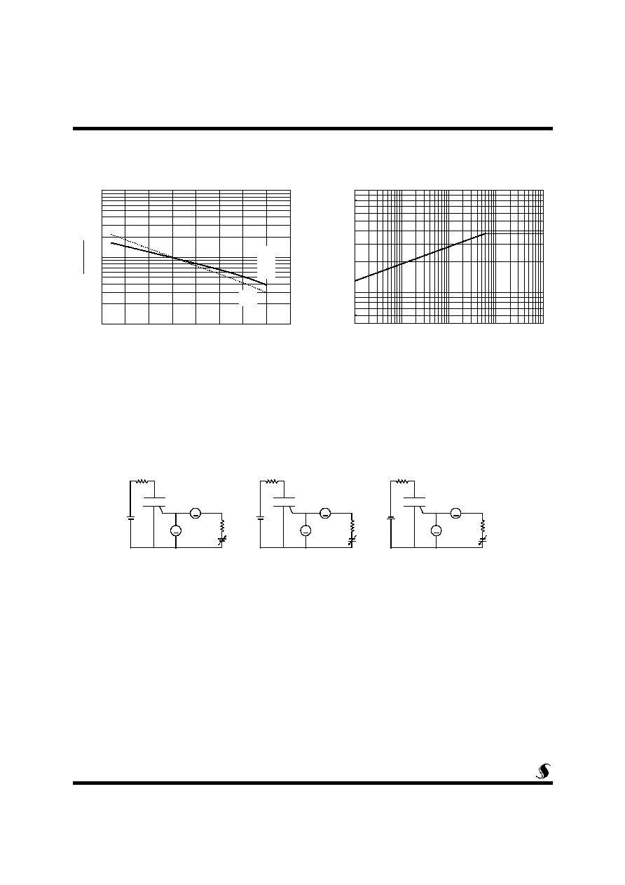
Fig 8. Transient Thermal Impedance
Fig 7. Gate Trigger Current vs.
Junction Temperature
Fig 9. Gate Trigger Characteristics Test Circuit
A
V
10
6V
R
G
A
V
10
6V
R
G
A
V
10
6V
R
G
Test Procedure
Test Procedure
Test Procedure
STF6A60