Absolute Maximum Ratings
( T
J
= 25∞C unless otherwise specified )
Symbol
Parameter
Condition
Ratings
Units
V
DRM
Repetitive Peak Off-State Voltage
600
V
I
T(RMS)
R.M.S On-State Current
T
C
= 86 ∞C
25
A
I
TSM
Surge On-State Current
One Cycle, 50Hz/60Hz, Peak,
Non-Repetitive
225/250
A
I
2
t
I
2
t
260
A
2
s
P
GM
Peak Gate Power Dissipation
5.0
W
P
G(AV)
Average Gate Power Dissipation
0.5
W
I
GM
Peak Gate Current
2.0
A
V
GM
Peak Gate Voltage
10
V
T
J
Operating Junction Temperature
- 40 ~ 125
∞C
T
STG
Storage Temperature
- 40 ~ 150
∞C
Mass
6.2
g
Oct, 2002. Rev. 1
Features
Repetitive Peak Off-State Voltage : 600V
R.M.S On-State Current ( I
T(RMS)
= 25 A )
High Commutation dv/dt
General Description
This device is suitable for AC switching application, phase
control application such as fan speed and temperature mod-
ulation control, lighting control and static switching relay.
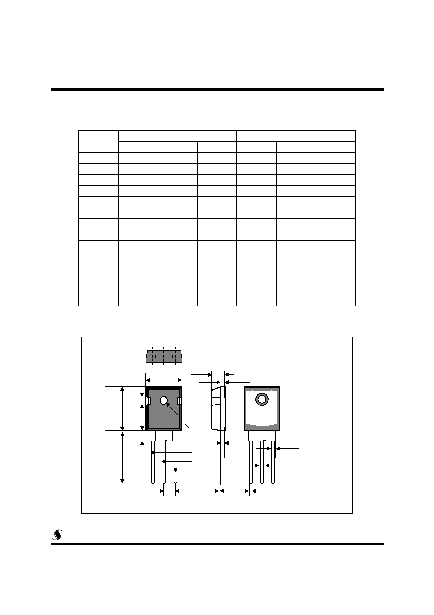
2.T2
3.Gate
1.T1
Symbol
TO-247
1
2 3
1/5
STW25A60
SemiWell
Semiconductor
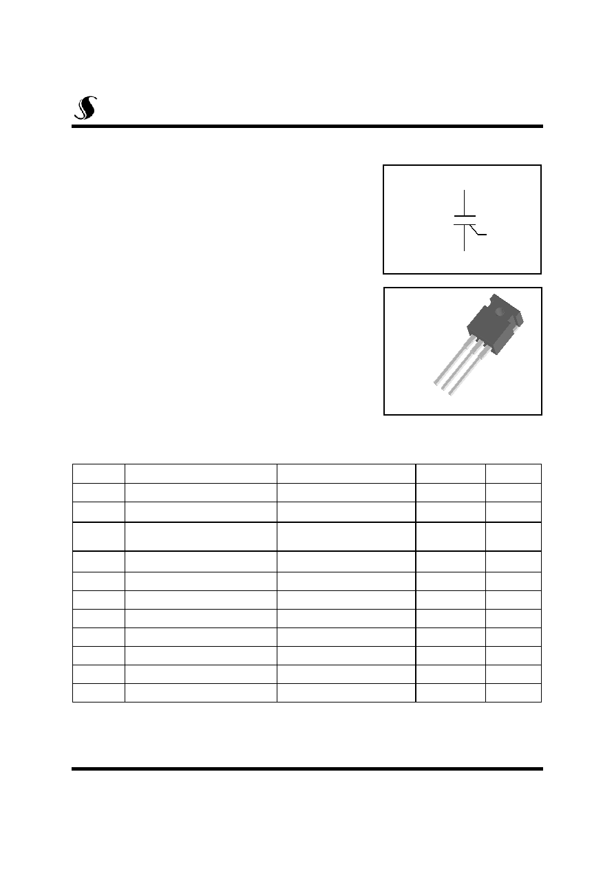
Bi-Directional Triode Thyristor
Copyright@SemiWell Semiconductor Co., Ltd., All rights reserved

Electrical Characteristics
Symbol
Items
Conditions
Ratings
Unit
Min.
Typ.
Max.
I
DRM
Repetitive Peak Off-State
Current
V
D
= V
DRM
, Single Phase, Half Wave
T
J
= 125 ∞C
5.0
mA
V
TM
Peak On-State Voltage
I
T
= 35 A, Inst. Measurement
1.4
V
I
+
GT1
Gate Trigger Current
V
D
= 6 V, R
L
=10
30
mA
I
-
GT1
30
I
-
GT3
30
V
+
GT1
Gate Trigger Voltage
V
D
= 6 V, R
L
=10
1.5
V
V
-
GT1
1.5
V
-
GT3
1.5
V
GD
Non-Trigger Gate Voltage
T
J
= 125 ∞C, V
D
= 1/2 V
DRM
0.2
V
(dv/dt)c
Critical Rate of Rise Off-State
Voltage at Commutation
T
J
= 125 ∞C, [di/dt]c = -12.5 A/ms,
V
D
=2/3 V
DRM
6
V/
I
H
Holding Current
35
mA
R
th(j-c)
Thermal Impedance
Junction to case
1.3
∞C/W
STW25A60
2/5
-50
0
50
100
150
0.1
1
10
V
+
GT1
V
_
GT1
V
_
GT3
V
GT
(t
o
C)
V
GT
(2
5
o
C)
Junction Temperature [
o
C]
10
0
10
1
10
2
0
40
80
120
160
200
240
280
60Hz
50Hz
Surg
e O
n
-
S
t
a
t
e
Cur
ren
t
[
A
]
Time (cycles)
0
5
10
15
20
25
30
80
90
100
110
120
130
= 90
o
= 150
o
= 60
o
= 30
o
= 180
o
= 120
o
Al
low
able
Case
T
e
mp
erat
ure
[
o
C]
RMS On-State Current [A]
0
5
10
15
20
25
30
0
5
10
15
20
25
30
35
= 90
o
= 150
o
= 60
o
= 30
o
= 180
o
= 120
o
Pow
e
r Di
s
s
ipat
i
on [
W
]
RMS On-State Current [A]
0.5
1.0
1.5
2.0
2.5
3.0
3.5
10
0
10
1
10
2
10
3
T
J
= 125
o
C
T
J
= 25
o
C
On-State
C
u
r
r
e
n
t
[
A
]
On-State Voltage [V]
10
1
10
2
10
3
10
-1
10
0
10
1
V
GD
(0.2V)
I
GM
(2
A
)
25
P
G(AV)
(0.5W)
P
GM
(5W)
V
GM
(10V)
Ga
t
e
V
o
l
t
age
[V
]
Gate Current [mA]
STW25A60
3/5
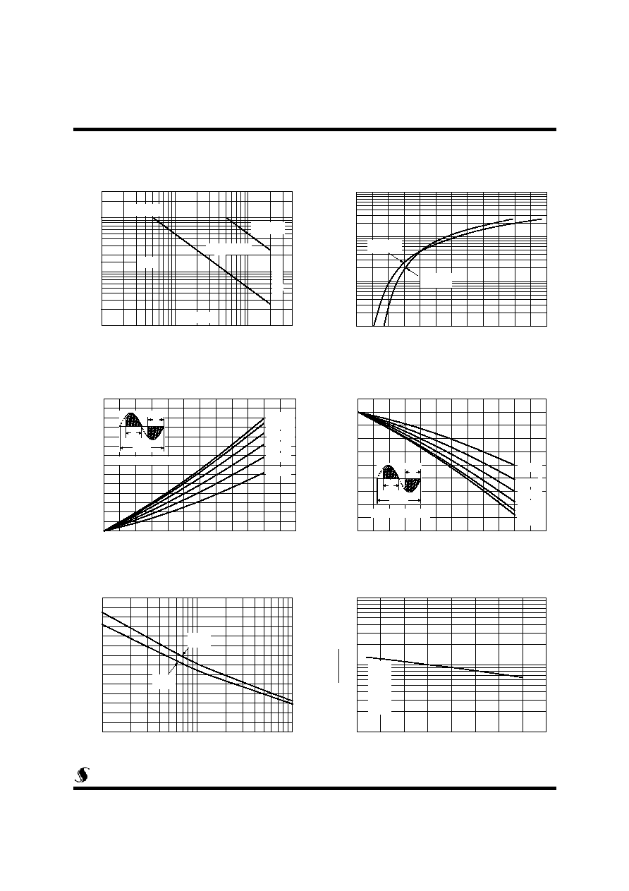
Fig 1. Gate Characteristics
Fig 2. On-State Voltage
Fig 3. On State Current vs.
Maximum Power Dissipation
Fig 4. On State Current vs.
Allowable Case Temperature
Fig 5. Surge On-State Current Rating
( Non-Repetitive )
Fig 6. Gate Trigger Voltage vs.
Junction Temperature
2
360∞
: Conduction Angle
2
360∞
: Conduction Angle
-50
0
50
100
150
0.1
1
10
I
_
GT3
I
+
GT1
I
_
GT1
I
GT
(t
o
C)
I
GT
(2
5
o
C)
Junction Temperature [
o
C]
10
-2
10
-1
10
0
10
1
0.1
1
10
T
r
ansi
e
nt T
h
ermal
Impe
da
nce
[
o
C/
W
]
Time (sec)
4/5
STW25A60
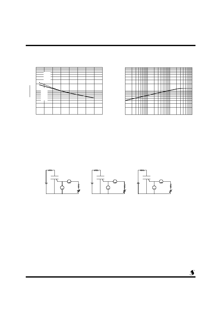
Fig 8. Transient Thermal Impedance
Fig 7. Gate Trigger Current vs.
Junction Temperature
Fig 9. Gate Trigger Characteristics Test Circuit
A
V
10
6V
R
G
A
V
10
6V
R
G
A
V
10
6V
R
G
Test Procedure
Test Procedure
Test Procedure