Äîêóìåíòàöèÿ è îïèñàíèÿ www.docs.chipfind.ru
1
2
Advanced Communications
ACS104A Data Sheet
Description
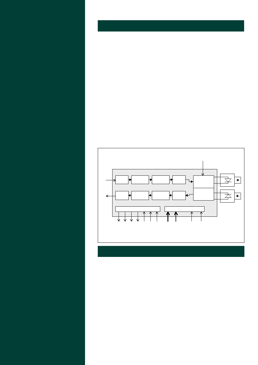
Equivalent Block Diagram of ACS104A
ACS104A
*
Low cost, single-chip solution for data powered RS-232 modems
using twin fiber-optic cables. Includes all analog/digital functions
except for power extraction circuitry and RS-232 level shifting.
*
Suitable for plastic or glass fiber, RF, infra-red over free air or
other media.
*
Uses low cost LED and PIN combination to transmit and receive
data.
*
Additional operating mode to support PIN with integrated TIA.
*
Asynchronous data rates from DC to 162kbps.
*
Very low power consumption; typically 2 - 3mA, which could be
extracted from the RS232 port itself, for > 12 dB link budget.
*
Supports 3 additional low frequency asynchronous channels or
the RS-232 handshake signals.
*
Bit Error Rate (BER) < 10
-9
*
Available in 44 pin TQFP (part no: ACS104A-TQ) and 28 pin
PLCC (part no: ACS104A-PL) packages.
The ACS104A is a complete controller, driver and receiver IC, supporting full-
duplex asynchronous transmission from DC to 162kbps over a serial link.
Improved sensitivity and additional operating modes are offered over the
ACS104. Although primarily designed to be used with standard LED emitters and
PIN receivers and twin optical fibers, any other simple serial media may be used.
The ACS104A is optimised for very low power consumption, consuming only 2 -
3mA at RS-232 data rates including power provided to the LED and 'heartbeat'
monitor. In applications where the power is extracted from the RS232 data lines,
this leaves a generous amount of power left for any power extraction and RS-232
level shifting circuitry.
The ACS104A employs data compression and time compression techniques,
affording high launch power in short bursts, leading to a low average power
consumption. The advantage of this approach is that high link budgets can be
achieved with inexpensive optical components. For example, the recommended
set-up for RS-232 applications (19.2kbps + handshake signals) assumes that the
LED is driven with a peak current of approximately 15.4mA for 6 % of the time.
The machine cycle is short enough to facilitate power supply smoothing with a
small external capacitor in the region of 100µF.
LED
Driver
PIN
Receiver
Data
Compress
3B4B
Encoder
Digital
Filter
Data
Decompress
3B4B
Decoder
Digital
Filter
RS-232 Interface
Control Logic
DCDB CTS
DSR
RTS
DTR
DR(2:1) DM(2:1)
LED/PIN
combinations
TRC
TxD
RxD
FIFO Time
Decompress
FIFO Time
Compress
PORB
RIO
RII
HBT
100 SERIES
Features
ACS104A Fiber Modem
ACS104A Revision 1.6 September 2000

2
2
Advanced Communications
ACS104A Data Sheet
Dual Fiber Modem for Asynchronous Data Rates from DC to 160kbps
current. The current is controlled by a resistance Rtrc connected
between TRC and GND. The lower the value of Rtrc the greater
the current. The lower limit for Rtrc is 800
while a practical
maximum is 40
k
.
The LED current is inversely proportional to Rtrc while Rtrc > 800
.
LED current = (100 / Rtrc) +/- 25 %
Data-Rate Selection
The ACS104A benefits from data compression circuitry which
reduces power consumption and improves the BER (Bit Error
Rate). The compression technique employed, demands a
minimum TxD data-bit time of 10 sample-clocks. This defines the
maximum data rate:
Maximum data rate = sample-clock/10
However, an allowance must be made for any variation in the TxD
data-bit period to accommodate frequency variation and jitter.
Hence the maximum data rates specified in the following are
decreased by 10% to include a sufficient safety margin.
The ACS104A includes an input pulse shaper which ensures that
the system is very tolerant to jitter, and helps achieve a maximum
data-rate close to the theoretical maximum of sample-clock/10
(bps). The pulse shaper will expand data pulses of less than 10
clock-samples to meet the compression criteria. This is performed
on up to three consecutive data-bits which fail to meet the
minimum pulse width criteria.
DR3
DR2
DR1 XTAL Sample Max TxD
Clock Clock Data Rate
0
1
1
10MHz
XTAL/160 5.6kbps
1
0
0
10MHz
XTAL/80
11kbps
1
0
1
10MHz
XTAL/40
22kbps
1
1
0
10MHz
XTAL/20
45kbps
1
1
1
10MHz
XTAL/15
60kbps
1
1
1
20MHz
XTAL/15
120kbps
1
1
1
27MHz
XTAL/15
162kbps
Table 1. TxD Data-Rate Selection
Table 1. shows the maximum TxD data rate, which includes a 10%
tolerance margin, when using various frequency crystals, other
sample-clock frequencies may be generated by using the
appropriate value XTAL in combination with the divide constant
selected by DR(1:3) namely 15, 20, 40, 80 or 160. The advantage
of using a slower crystal and a lower sample clock is the reduced
power consumption of the device.
DR3 is internally held high in the PLCC28 package.
RS-232 Handshake Signals / Low Frequency Data Channels
Three additional low frequency data channels are provided on the
ACS104A which are often used for the RS-232 handshake signals.
The RS-232 handshake signals comprise the set RTS, CTS, DTR
and DSR. These are treated as pass through data channels rather
than using local handshaking. Hence the status of inputs RTS and
DTR appear at the far-end outputs CTS and DSR respectively. An
extra data channel has also been provided in the TQFP44
package, which may be used for sending the RS232 Ring Indicator
signal, for example. The input and output lines are RII and RIO
respectively.
The transmission method employed on the ACS104A has been
designed to give low skew (1 - 2 data-bits) on the main RTS, CTS,
DTR and DSR hanshake signals relative to the main TxD/RxD data
channel, while maintaining low power consumption.
The handshake signals are updated by two stimuli:
i.
An internal interval timer at a frequency proportional to the XTAL; at
10.0MHz this is approximately 1.6ms.
ii.
Changes detected on RTS and DTR.
The maximum bandwidth for the handshake signals may be
Transmitter and Receiver Functions
This device offers one high speed and three low speed full duplex
channels to the user in a completely transparent way, appearing as
4 full duplex channels.
Data from the TxD and low frequency channels is time
compressed in an internal FIFO and sent over the fiber link in a
burst within a predefined window. The two devices at each end of
the link automatically synchronise with each other such that the
transmit and receive windows are interleaved. This technique
offers superior performance compared to continuous receive and
transmit systems, since the transmitted data does not cause noise
injection during the receiving time. The TxD input data of the
transmitting modem is also data compressed. The 3B4B encoding
method is used for communication between ACS104As, thus
ensuring that there is no DC component in the signal. The
encoding and decoding is transparent to the user.
In the receiving modem, 3B4B encoding ensures easy extraction of
the bit-clock. The received data is filtered, decoded, and then
stored in the output memory. The memory provides time
expansion, de-jittering and frequency compensation functions. The
data is then decompressed and directed to the RxD output pin,
appearing after a minimal delay, in the same format as that
presented at the TxD pin at the far end.
Operational Modes
The ACS104A is compatible with the ACS104 but offers over twice
the max data rate. The following sections detail the operating
modes. Additional modes are also described for new ways of
interfacing the device with external PIN / amplifier modules. The
setups refer to the pin settings for the TQFP44 package. The
PLCC28 pin settings will be the same with the unavailable pins
being internally pulled high.
Mode 1 - Dual Fiber LED/PIN mode
Setup : DP4=1, DP3=1, DP2=1, DP1=1
This is a twin-fiber mode where the LED is used for transmission
and a separate PIN Diode is used for reception. An example circuit
diagram showing the necessary connections is shown in figures 3
and 4.
Mode 2 - Preamp Voltage Input & LED Drive
Setup : DP4=0, DP3=1, DP2=0, DP1=0, NSB=0 (TQFP44 only)
This is a mode for use with external amplifier and PIN modules. An
LED is used for transmission and connected as normal with its
anode to LAP and cathode to LAN. The differential voltage from
an external PIN/TIA module is connected to PINN and PINP via
100pF capacitors to provide DC isolation. The signals should be
connected such that PINP is connected to the TIA output that goes
high when light is received. A single input can also be applied from
a single ended PIN/TIA by feeding the input to PINP only, PINN is
left floating. This mode uses the new NSB pin, in all other modes
this pin should be left disconnected or connected to VA+.
Mode 11 - Digital Data Input & LED Drive
Setup : DP4=1, DP3=0, DP2=1, DP1=0
This is a mode for use with external amplifier and PIN modules that
provide fully digital output levels. An LED is used for transmission
and connected as normal as shown in figure 4. The output from an
external PIN/TIA module is connected to CNT. The polarity of the
input should be such that CNT that goes high when light is
received.
LED current control
The LED transmit current is not critical though it is important not to
exceed the LED manufacturer's recommendation for maximum

3
2
Advanced Communications
ACS104A Data Sheet
programmed using pins HD(1:2) on the TQFP44 package, in
accordance with the Table 2.
HD2
HD1
Handshake
Skew
Bandwidth
w.r.t. RxD
0
0*
600
Hz
10 ms.
0
1
10
kHz
1 - 2 data bits
1
0
5
kHz
1 - 2 data bits
1
1
2.5
kHz
1 - 2 data bits
Table 2. Handshake signal bandwidth allocation
* When HD2 = HD1 = 0 super-compress mode is selected. See
section headed Super-Compress mode.
Handshake data rates which exceed the allocated bandwidth will
be delayed, and consequently result in additional skew between
handshake signals and data.
The HD pins enable the user to allocate a maximum bandwidth to
the handshake signals and thus limit the power consumption of the
device. The power consumption is, however, dependent on the
actual bandwidth used and not the bandwidth selected. For
example; if the handshake signals were toggled at 1kHz the power
consumption would be the same for an allocated bandwidth of
2.5kHz as it would for an allocation of 10kHz. See section headed
Current and Power Consumption for more details.
Super-Compress mode
This mode is selected when HD2 = HD1 = 0. Super-compress
mode performs a second stage of data compression, thus further
reducing the power consumption of the modem. Normally, data is
compressed in a manner which is independent of the data type. In
super-compress mode, an additional stage of compression further
reduces the data by a factor of 1 to 3 depending on the data itself.
Example: The super-compress stage will compress DC data by an
additional Compression Factor (CF) of 3, whilst data close to the
maximum frequency will not be compressed beyond the standard
CF of 1.
Super-compress mode provides benefits where the user is
interested in low average power consumption (e.g. battery life)
rather than peak power. If the intended system is idle for most of
the time with periodic bursts of activity, the additional data
compression afforded will approach a CF of 3.
Locking
To achieve low power consumption the ACS104A is active for a
small percentage of the frame (machine-cycle) known as the
'transmit' window and the 'receive' window, collectively these
windows are known as the 'active time'. Outside the 'active time'
the device is largely dormant accept for the maintenance of the
oscillator and basic 'house-keeping' functions.
Communicating modems attain a stable state known as 'locked',
where the 'transmit' window of one modem coincides with the
'receive' window of the other, allowing for the delay through the
optical link. Adjustments to machine cycles are made
automatically during operation, to compensate for differences in
XTAL frequencies which cause loss of synchronisation.
The ACS104A locking algorithm is statistical, and consequently the
locking time will differ on each attempt to lock.
Diagnostic and Locking Modes
The diagnostic and operational modes, shown in Table 3, are
selected using the DM pins. DM3 is held high internally on the
PLCC28 package.
DM3
DM2
DM1
Mode
Lock
0
0
0
Full-duplex
Drift
0
0
1
Full-duplex
Active
0
1
0
Full-duplex
Memory
1
0
1
Local loopback
Random
1
1
0
Remote loopback
Random
1
1
1
Full-duplex
Random
Table 3. Diagnostic and operational modes
Local Loopback
In local loopback mode TxD data is looped back inside the near-end
modem and appears at its own RxD output. RTS, DTR and RII are
also looped back appearing at their own CTS, DSR and RIO outputs
respectively. The data is also sent to the far-end modem and
synchronisation between the modems is maintained.
In local loopback mode data received from the far-end device is
ignored, except to maintain lock. If concurrent requests occur for
local and remote loopback, local loopback is selected.
The local loopback diagnostic mode is used to test data flow up to,
and back from, the local ACS104A and does not test the integrity of
the link itself, i.e. local loopback operates independently of
synchronisation with a second modem.
Remote Loopback
In remote loopback mode, the near-end modem sends a request to
the far-end modem to loopback its received data, thus returning the
data so that it appears at the RxD of the initiating modem. RTS,
DTR and RII follows the same path, returning data back to CTS,
DSR and RIO respectively of the initiating modem. Data also
appears at the far-end modem outputs RxD, CTS, DSR and RIO. In
the process both modems are exercised completely, as well as the
LED/PINs and the fiber optic link. The remote loopback test is
normally used to check the integrity of the entire link from the near-
end (initiating) modem. Whilst a device is responding to a request
for remote loopback from the initiating modem (far-end), requests to
initiate remote loopback will be ignored.
Drift lock
Communicating modems attain a stable state where the 'transmit'
window of one modem coincides with the 'receive' window of the
other, allowing for delay through the optical link. Adjustments to
machine cycles are made automatically during operation to
compensate for differences in XTAL frequencies which would
otherwise cause loss of synchronisation.
Using drift lock, synchronisation described above depends on a
difference in the XTAL frequencies at each end of the link, and the
greater the difference the faster the locking. Therefore, if the
difference between XTAL frequencies is very small (a few ppm),
automatic locking may take tens of seconds or even minutes.
Drift lock will not operate if the two communicating devices are driven by
a clock derived from a single source (i.e. tolerance of 0ppm).
Active Lock Mode
Active lock mode may be used to accelerate synchronisation of a
pair of communicating modems. This mode synchronises the
modems in less than 3 seconds by adjusting the machine cycles of
the modems. Active lock reduces the machine cycle of the device
by 0.5 % ensuring rapid lock. After synchronisation the machine
cycle reverts automatically to normal.
Only one device may be configured in active lock mode at any one
time. Active lock mode is usually invoked temporarily on power-up.
This can be achieved on the ACS104A by connecting DM1 to an RC
arrangement, i.e. with the capacitor to 5V and the resistor to GND, to
create a 5V
à
0V ramp on power-up. The RC time constant should
be Ca. 5 seconds. Active lock will succeed even when
communicating devices are driven from clocks derived from a single
source (0ppm).
Random Lock
This mode achieves moderate locking times (typically 5 seconds,
worst case 10 seconds) with the advantage that the ACS104A's are
configured as peers. Communicating modems may be permanently
configured in this mode by hard wiring the DM pins.
Random lock will succeed even when communicating devices are
driven from clocks derived from a single source (0ppm). Random
lock mode is compatible with drift lock and active lock.
Memory Lock
Following the assertion of a reset (PORB = 0) communicating
devices will initiate an arbitration process where within 10 seconds

4
2
Advanced Communications
ACS104A Data Sheet
the communicating modems will achieve synchronisation with one
establishing itself as an active lock modem and the other
establishing itself as a drift lock modem. On subsequent attempts to
lock, synchronisation will be achieved within 3 seconds. It is only
necessary to apply reset to one device in the communicating pair to
initiate an arbitration process.
Since memory lock uses on-chip storage, loss of power to the
modem will require a new reset (PORB=0). Furthermore, should
there be a need to synchronise with a third modem a reset will again
be required.
Mixing Lock modes
It is possible to mix all combinations of locking modes once the
modems are locked, however, prior to synchronisation two modems
configured in active lock will not operate. The effect of mixing
locking modes on locking speed is given in Table 4 :
Device A
Device B
Locking Speed
Mode
Mode
Drift
Drift
Drift
Drift
Active
Active
Drift
Random
Random
Drift
Memory
Random
Active
Active
Not allowed
Active
Random
Random
Active
Memory
Random
Random
Random
Random
Random
Memory
Random
Memory
Memory
Active
(Random on first synchronisation)
Table 4. Mixing lock modes
PORB
The Power-On Reset or PORB resets the device if forced Low for
100ms or more. This pin should be connected as figure 4.
Crystal Clock
Normally, a parallel resonant crystal will be connected between the
pins XLI and XLO with the appropriate padding capacitors. The
crystal oscillator will operate with padding capacitors of value 0 -
50pF, and the designer should endeavour to use padding capacitors
of low value since this will ensure the lowest power consumption.
The ACS104A has been designed to operate with a crystal tolerance
of +/- 250ppm giving a relative tolerance between communicating
modem pairs of 500 ppm. This wide tolerance will support the use of
low value padding capacitors.
Alternatively, XLI may be driven directly by an external clock. The
clock frequency for the purpose of this specification is referred to as
the XTAL frequency. The operational range for the XTAL frequency
is 5 - 27MHz, though communicating devices must use the same
nominal value.
DCDB
The Data Carrier Detect (DCDB) signal goes Low when the modems
are synchronised ('locked') and ready for data transmission. Prior to
lock (DCDB = High), the data channel output RxD will be forced Low
and the handshake outputs CTS and DSR will be forced High.
The status of DCDB is also given by the HBT pin. See section
headed HBT Status pin.
CNT Capacitor
The CNT value is inversely proportional to the XTAL frequency. The
capacitor is connected between pins CNT and GND. A 20 %
tolerance on CNT is sufficient. For a XTAL frequency range of
5 to 27MHz the recommended value of the capacitor on CNT is from
47nF at 5MHz, 22nF at 10Hz down to 10nF at 27MHz . A ceramic
type is required to ensure low leakage. The CNT capacitor value
has an effect on the initial locking time and the receiver sensitivity
limit. Higher values giving improved sensitivity and lower values
giving faster locking.
ERL (Error Detector)
This signal can be used to give an indication of the quality of the
optical link. Even when a DC signal is applied to the data and
handshake inputs, the ACS104A modem transmits up to 200kbps
over the link in each direction. This control data is used to maintain
the timing and the relative positioning of 'transmit' and 'receive'
windows.
The transmit and control data is constantly monitored to make sure it
is compatible with the 3B4B format. If a coding error is detected,
ERL will go High and will remain High until reset. ERL may be reset
by asserting PORB, or by removing the fiber-optic cable from one
side of the link thereby forcing the device temporarily out of lock.
Please note that ERL detects coding errors and not data errors,
nevertheless because of the complexity of the coding rules on the
ACS104A the absence of detected errors on this pin will give a good
indication of a high quality link.
HBT Status pin ('Heartbeat' Indicator LED)
The ACS104A HBT pin affords a method of driving a display LED in
a manner which is sympathetic to low power consumption. The HBT
pin is pulsed to indicate 'locked' status (DCDB = 0) and 'out of lock'
status (DCDB =1). The frequency of pulses is 8 times greater for
'out of lock' than for 'lock'. The LED 'on' indicates power-up whilst
the frequency of pulsing denotes locking status.
Since the display LED is on for (at most) 3.2 % of the total time, the
HBT requires little power which may be further reduced by
employing high efficiency LEDs.
Powered-up, but not locked
Frequency (Hz):
XTAL / 3.89 * 10
6
Duration (s):
61,440 / XTAL
On time (%):
3.2 % of time.
With 10MHz XTAL :
Frequency:
2.5Hz (approx.)
Duration:
6.1ms (approx.)
Powered-up and locked
Frequency (Hz):
XTAL / 15.36 * 10
6
Duration (s):
61,440 / XTAL
On time (%):
0.4 % of time.
With 10MHz XTAL :
Frequency:
0.65Hz (approx.)
Duration:
6.1ms (approx.)
The HBT pin is active High and can supply up to 16mA at a voltage
of > VDD - 0.5 Volts. The display LED should be placed between
the HBT pin and GND with a series resistor. The resistor value is a
function of the efficiency of the display LED, and the power budget.
Example: Calculating the HBT resistor value
LED on voltage:
2.0V
VDD (ACS104A):
5.0V
Resistor voltage:
3.0V
Current to LED:
2 mA (high efficiency LED)
Resistor value:
3/2*10
-3
= 1500
Average current:
64µA
Average power:
0.32mW
Note: The LED referred to in this section is of the inexpensive
display type and should not be confused with the LED that
interfaces with the fiber optic cable itself.
Power consumption considerations
The power consumption of the ACS104A is a function of the
following:
i.
The sample-clock DR(1:3)
ii.
The transmit current setting (TRC)
iii.
Handshake signals frequency
iv.
XTAL frequency
v.
Supply voltage
The sample-clock
The sample-clock selected by DR(1:3), see section headed Data-
Rate Selection, determines the quantity of data transmitted over
the fiber link. The 'transmit' window opens once each frame and
closes when the time compress FIFO is empty. The 'receive'
window is aligned with the 'transmit' window of the far-end modem,
and tracks the 'transmit' window such that it closes on detection of
the last data bit. Clearly, the lower the sample-clock the smaller
the active time and the lower the power consumption.
The transmit current setting
The formula given in section headed LED current control, relates to
the peak current delivered to the LED. The average current

5
2
Advanced Communications
ACS104A Data Sheet
however is very much lower. The DC balanced nature of data
encoding means the LED consumes current for approximately
50 % of the 'transmit' window time. The average current delivered
to the LED is therefore a function of both the peak current and the
duration of the 'transmit' window.
Handshake signals frequency
Handshake data which is interleaved with the main data channel is
generated and written to the time compress FIFO each time a
change is detected on either RTS or DTR. The power consumption
is lower when the signals change at low frequency or are held at a
DC level. It is possible to limit the power consumption dedicated to
the handshake signals by limiting the frequency of operation using
HD(1:2) input pins. See section headed RS-232 Handshake
Signals.
XTAL frequency
The ACS104A uses CMOS technology and therefore the power
consumption is proportional to the frequency of switching.
Consequently, the effect of reducing the value of the XTAL alone
will result in lower power consumption. However, the current
component delivered to the LED and sourced from outputs such as
RxD and HBT are static and as such are independent of the XTAL
frequency.
It is worth noting that a modem pair configured with an XTAL of
10MHz and a sample-clock of XTAL/40 will yield the same
performance as a modem pair configured with an XTAL of 5MHz
and a sample-clock of XTAL/20. However, the modem pair with the
lower value XTAL is likely to consume the higher power with a
higher data delay (see section headed Data delay and skew). This
is because, although the dynamic power has reduced, the higher
sample-clock leads to a much longer active time, a factor which
dominates the overall power calculation.
Supply voltage
The ACS104A has been designed to operate over the voltage
range 3.3 Volts to 5.25 Volts. For the purpose of this specification
the power consumption figures presume a worst case supply of
5.25 Volts. It is anticipated that there will be a significant
reduction in power consumption where the device is operated at
lower voltages.
Current and Power Consumption
The average current consumption may be split into two
components; the dynamic component and the static component.
The dynamic component is dependent on the XTAL frequency
while the static component is dependent on static current loads.
(See Calculating average current and power consumption for
details).
Since the peak current can be very much greater than the
average current, it is important to use a substantial smoothing
capacitor on VA+ and VD+. The recommended values are at
least 47µF
*
for VD+ and 100µF
*
for VA+. The configuration can be
seen in Figure 1. (* Capacitor tolerance +/- 20 %)
Data delay and skew
The Full Duplex Delay (FDD) through the system, which applies to
TxD
à
RxD, RTS
à
CTS and DTR
à
DSR, is shown in Table 5.
DR3
DR2
DR1
FDD
0
1
1
6.5ms
1
0
0
3.8ms
1
0
1
2.8ms
1
1
0
2.3ms
1
1
1
2.0ms
Table 5. FDD with XTAL = 10MHz
The FDD is inversely proportional to the XTAL frequency and may
be calculated for other XTALs using the formula below:
FDD
XTAL
= (10
7
/ XTAL) * FDD
10MHz
The skew between the main TxD data channel and handshake
signals is 1 - 2 data bits as long as the maximum handshake data-
rate of 2kbps is respected. For handshake frequencies above
2kbps, the skew will be proportional to the handshake signal
frequency.
LED considerations & Suppliers
Since LEDs from different suppliers may emit different
wavelengths, it is recommended that the LEDs in a
communicating pair of modems are obtained from the same
supplier. The ACS104A can support any wavelength LED or
LASER. Furthermore, the emission spectrum is a function of
temperature, so a temperature difference between the ends of a
link reduces the responsivity of the receiving LED, resulting in a
reduction in the link budget. Information is given in the suppliers'
data sheets. The following manufacturers have components that
will be tested with the ACS104A and Acapella will be glad to
assist with contact names and addresses on request:
HP
Rohm
Mitsubishi
Optek Technology
AMP/Lytel
MITEL
OKI
UTP
Honeywell
Power Supply Decoupling
The ACS104A contains a highly sensitive amplifier, capable of
responding to extremely low current levels. To exploit this
sensitivity it is important to reduce external noise to a low level
compared to the input signal from the LED or PIN. The modem
should have an independent power trace to the point where
power enters the board.
Figures 3 to 4 show the recommended power supply decoupling.
The LED and PIN should be sited very close to the PINP, PINN,
LAN and LAP pins. A generous ground plane should be
provided, especially around the sensitive PINP, PINN, LAN and
LAP pins. The modem should be protected from EMI/RFI
sources in the standard ways.
Link Budgets
The link budget is the difference between the power coupled to
the fiber via the transmit LED and the power required to realise
the minimum input-amplifier current via the receive LED/PIN.
The link budget is normally specified in dB or dBm, and
represents the maximum attenuation allowed between
communicating LEDs. The budget is utilised in terms of the cable
length, cable connectors and splices. It usually includes an
operating margin to allow for degradation in LED performance.
The power coupled to the cable, is a function of the efficiency of
the LED, the current applied to the LED and the type of the fiber
optic cable employed. The conversion current produced by the
reverse biased LED is a function of the LED efficiency and the
fiber type.
Power extraction from RS232 Data lines
The power supply requirements of the ACS104A have been
designed to be low enough so that no external power supply is
required. Instead the current required to supply the device can be
extracted from the RS232 data lines. Figure 5 illustrates a possible
application circuit that may be used to extracted enough power
from the RS232 data input signals to power the Acapella IC and
the optics and to drive back the RS232 output signals, in order to
provide a full duplex RS232 link. In the system described, three
input data lines are used for power extraction : TxD, RTS and DTR.
In the application circuit illustrated, only the RxD and CTS interface
signals are driven back again to the port, with the DCD (data
carrier detect) and DSR (data set ready) signals permanently
activated by being tied to the positive supply. Data communication
is then possible using all communication protocols, including
hardware handshaking, with communication under the control of
RTS and CTS. If required the DCD and DSR signals could be
actively driven from the Acapella I.C. via another switching device
or dedicated line driver. Alternatively these could be disconnected
to reduce the current extraction requirements.