Revision 3.01/October 2003 © Semtech Corp.
Page 1
www.semtech.com
ACS8520 SETS
ADVANCED COMMUNICATIONS
FINAL
Synchronous Equipment Timing Source for
Stratum 3/4E/4 and SMC Systems
ADVANCED COMMUNICATIONS
FINAL
DATASHEET
The ACS8520 is a highly integrated, single-chip solution
for the Synchronous Equipment Timing Source (SETS)
function in a SONET or SDH Network Element. The device
generates SONET or SDH Equipment Clocks (SEC) and
Frame Synchronization clocks. The ACS8520 is fully
compliant with the required international specifications
and standards.
The device supports Free-run, Locked and Holdover
modes. It also supports all three types of reference clock
source: recovered line clock, PDH network, and node
synchronization. The ACS8520 generates independent
SEC and BITS/SSU clocks, an 8 kHz Frame
Synchronization clock and a 2 kHz Multi-Frame
Synchronization clock.
Two ACS8520 devices can be used together in a Master/
Slave configuration mode allowing system protection
against a single ACS8520 failure.
A microprocessor port is incorporated, providing access to
the configuration and status registers for device setup
and monitoring. The ACS8520 supports IEEE 1149.1
[5]
JTAG boundary scan.
The user can choose between OCXO or TCXO to define the
Stratum and/or Holdover performance required.
Suitable for Stratum 3, 4E, 4 and SONET Minimum
Clock (SMC) or SONET/SDH Equipment Clock (SEC)
applications
Meets Telcordia 1244-CORE
[19]
Stratum 3 and
GR-253
[17]
, and ITU-T G.813
[11]
Options
and
specifications
Accepts 14 individual input reference clocks, all with
robust input clock source quality monitoring.
Simultaneously generates nine output clocks, plus
two Sync pulse outputs
Absolute Holdover accuracy better than 3 x 10
-10
(manual), 7.5 x 10
-14
(instantaneous); Holdover
stability defined by choice of external XO
Programmable PLL bandwidth, for wander and jitter
tracking/attenuation, 0.1 Hz to 70 Hz in 10 steps
Automatic hit-less source switchover on loss of input
Microprocessor interface - Intel, Motorola, Serial,
Multiplexed, or boot from EPROM
Output phase adjustment in 6 ps steps up to ±200 ns
IEEE 1149.1 JTAG Boundary Scan
Single 3.3 V operation. 5 V tolerant
Available in LQFP 100 package
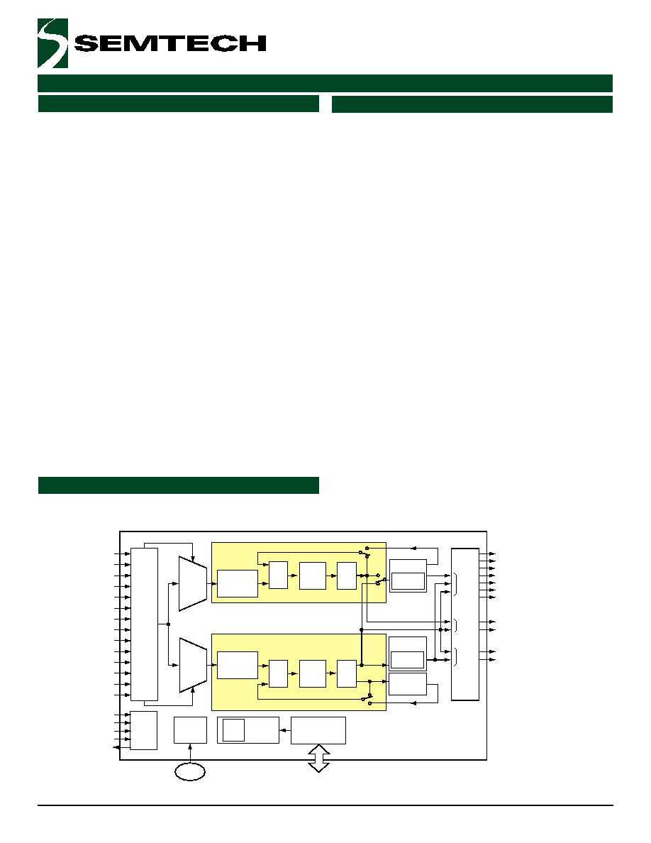
Figure 1 Block Diagram of the ACS8520 SETS
Block Diagram
Description
Features
IEEE
1149.1
JTAG
Input
Port
Monitors
and
Selection
Control
14 x SEC
Optional
Divider, 1/n
n = 1 to 2
14
Optional
Divider, 1/n
n = 1 to 2
14
PFD
Digital
Loop
Filter
Chip
Clock
Generator
DTO
TCK
TDI
TMS
TRST
TDO
F8520P_001BLOCKDIA_03
T4
Selector
T0
Selector
PFD
Digital
Loop
Filter
DTO
T4 APLL
Frequency
Dividers
T0 APLL
(output)
Frequency
Dividers
TO APLL
(feedback)
TO8
&
TO9
TO10
&
TO11
TO1
to
TO7
Outputs
T01-TO7:
E1/DS1 (2.048/
1.544 MHz)
and frequency
multiples:
1.5 x, 2 x, 3 x
4 x, 6 x, 12 x
16 x and 24 x
E3/DS3
2 kHz
8 kHz
and OC-N* rates
OC-N* rates =
OC-1 51.84 MHz
OC-3 155.52 MHz
and derivatives:
6.48 MHz
19.44 MHz
25.92 MHz
38.88 MHz
51.84 MHz
77.76 MHz
155.52 MHz
311.04 MHz
T08: AMI
TO9: E1/DS1
2 x AMI
10 x TTL
2 x PECL/LVDS
Programmable;
64/8 kHz (AMI)
2 kHz
4 kHz
N x 8 kHz
1.544/2.048 MHz
6.48 MHz
19.44 MHz
25.92 MHz
38.88 MHz
51.84 MHz
77.76 MHz
155.52 MHz
TO10: 8 kHz
(FrSync)
TO11: 2 kHz
(MFrSync)
Output
Ports
Priority
Table
Register Set
Microprocessor
Port
OCXO or
TCXO
T4 DPLL/Freq. Synthesis
T0 DPLL/Freq. Synthesis

Table of Contents
Revision 3.01/October 2003 © Semtech Corp.
Page 2
www.semtech.com
ACS8520 SETS
Section
Page
ADVANCED COMMUNICATIONS
FINAL
DATASHEET
Description................................................................................................................................................................................................. 1
Block Diagram............................................................................................................................................................................................ 1
Features ..................................................................................................................................................................................................... 1
Table of Contents ...................................................................................................................................................................................... 2
Pin Diagram ............................................................................................................................................................................................... 4
Pin Description........................................................................................................................................................................................... 5
Introduction................................................................................................................................................................................................ 8
General Description................................................................................................................................................................................... 8
Overview .............................................................................................................................................................................................8
Input Reference Clock Ports .......................................................................................................................................................... 10
Locking Frequency Modes.................................................................................................................................................... 10
PECL/LVDS/AMI Input Port Selection.................................................................................................................................. 11
Clock Quality Monitoring................................................................................................................................................................. 12
Activity Monitoring ................................................................................................................................................................. 12
Frequency Monitoring ........................................................................................................................................................... 14
Selection of Input Reference Clock Source................................................................................................................................... 14
Forced Control Selection....................................................................................................................................................... 15
Automatic Control Selection ................................................................................................................................................. 15
Ultra Fast Switching .............................................................................................................................................................. 15
Fast External Switching Mode-SCRSW Pin .......................................................................................................................... 15
Output Clock Phase Continuity on Source Switchover ....................................................................................................... 16
Modes of Operation ........................................................................................................................................................................ 16
Free-run Mode ....................................................................................................................................................................... 16
Pre-locked Mode ................................................................................................................................................................... 16
Locked Mode ......................................................................................................................................................................... 16
Lost-phase Mode................................................................................................................................................................... 17
Holdover Mode ...................................................................................................................................................................... 17
Pre-locked2 Mode ................................................................................................................................................................. 19
DPLL Architecture and Configuration ............................................................................................................................................ 19
TO DPLL Main Features ........................................................................................................................................................ 20
T4 DPLL Main Features ........................................................................................................................................................ 20
TO DPLL Automatic Bandwidth Controls.............................................................................................................................. 20
Phase Detectors .................................................................................................................................................................... 21
Phase Lock/Loss Detection.................................................................................................................................................. 21
Damping Factor Programmability......................................................................................................................................... 21
Local Oscillator Clock ............................................................................................................................................................ 22
Output Wander ...................................................................................................................................................................... 23
Jitter and Wander Transfer ................................................................................................................................................... 25
Phase Build-out ..................................................................................................................................................................... 25
Input to Output Phase Adjustment....................................................................................................................................... 26
Input Wander and Jitter Tolerance....................................................................................................................................... 26
Using the DPLLs for Accurate Frequency and Phase Reporting ........................................................................................ 28
Configuration for Redundancy Protection ..................................................................................................................................... 29
Alignment of Priority Tables in Master and Slave ACS8520 .............................................................................................. 30
T4 Generation in Master and Slave ACS8520 .................................................................................................................... 30
Alignment of the Output Clock Phases in Master and Slave ACS8520............................................................................. 30
MFrSync and FrSync Alignment-SYNC2K............................................................................................................................. 31
Output Clock Ports .......................................................................................................................................................................... 32
PECL/LVDS/AMI Output Port Selection ............................................................................................................................... 32
Output Frequency Selection and Configuration .................................................................................................................. 32
Table of Contents

Revision 3.01/October 2003 © Semtech Corp.
Page 3
www.semtech.com
ACS8520 SETS
Section
Page
ADVANCED COMMUNICATIONS
FINAL
DATASHEET
Microprocessor Interface ....................................................................................................................................................................... 43
Introduction to Microprocessor Modes ......................................................................................................................................... 43
Motorola Mode ...................................................................................................................................................................... 44
Intel Mode.............................................................................................................................................................................. 46
Multiplexed Mode.................................................................................................................................................................. 48
Serial Mode............................................................................................................................................................................ 50
EPROM Mode......................................................................................................................................................................... 52
Power-On Reset............................................................................................................................................................................... 52
Register Map........................................................................................................................................................................................... 53
Register Organization ..................................................................................................................................................................... 53
Multi-word Registers ............................................................................................................................................................. 53
Register Access ..................................................................................................................................................................... 53
Interrupt Enable and Clear ................................................................................................................................................... 53
Defaults.................................................................................................................................................................................. 53
Register Descriptions ............................................................................................................................................................................. 57
Electrical Specifications ....................................................................................................................................................................... 133
JTAG ...............................................................................................................................................................................................133
Over-voltage Protection ................................................................................................................................................................133
ESD Protection ..............................................................................................................................................................................133
Latchup Protection........................................................................................................................................................................133
Maximum Ratings .........................................................................................................................................................................134
Operating Conditions ....................................................................................................................................................................134
DC Characteristics ........................................................................................................................................................................134
DC Characteristics: AMI Input/Output Port ....................................................................................................................... 138
Jitter Performance ........................................................................................................................................................................140
Input/Output Timing .....................................................................................................................................................................142
Package Information ............................................................................................................................................................................ 143
Thermal Conditions.......................................................................................................................................................................144
Application Information........................................................................................................................................................................ 145
References............................................................................................................................................................................................ 146
Abbreviations ........................................................................................................................................................................................ 146
Trademark Acknowledgements ........................................................................................................................................................... 147
Revision Status/History ....................................................................................................................................................................... 148
Notes ..................................................................................................................................................................................................... 149
Ordering Information ............................................................................................................................................................................ 150
Disclaimers....................................................................................................................................................................................150
Contacts.........................................................................................................................................................................................150
ADVANCED COMMUNICATIONS
FINAL
DATASHEET
Revision 3.01/October 2003 © Semtech Corp.
Page 5
www.semtech.com
ACS8520 SETS
Note...I = Input, O = Output, P = Power, TTL
U
= TTL input with pull-up resistor, TTL
D
= TTL input with pull-down resistor.
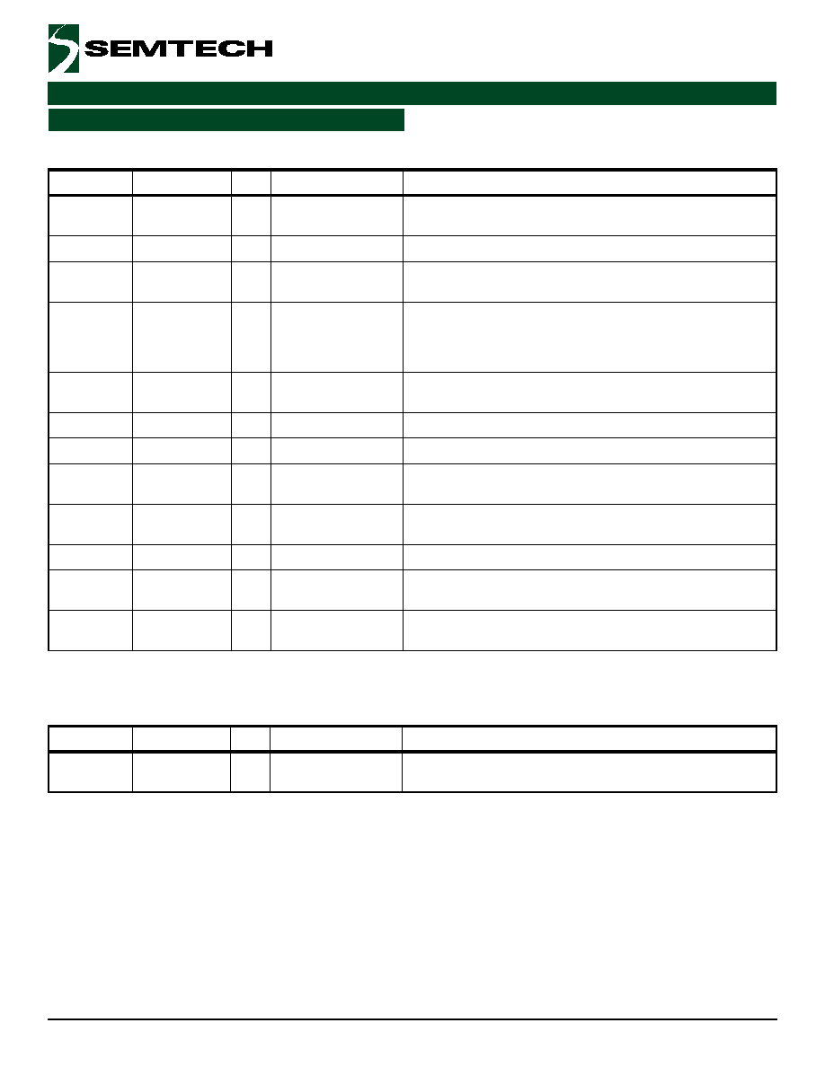
Pin Description
Table 1 Power Pins
Pin Number
Symbol
I/O
Type
Description
12, 13,
16
VD1+, VD3+,
VD2+
P
-
Supply Voltage: Digital supply to gates in analog section, +3.3 Volts
±10%.
26
VAMI+
P
-
Supply Voltage: Digital supply to AMI output, +3.3 Volts ±10%.
33,
39
VDD_DIFFa,
VDD_DIFFb
P
-
Supply Voltage: Digital supply for differential ports, +3.3 Volts ±10%.
44
VDD5
P
-
Digital Supply for +5 Volts Tolerance to Input Pins. Connect to +5 Volts
(±10%) for clamping to +5 Volts. Connect to VDD for clamping to +3.3
Volts. Leave floating for no clamping, input pins tolerant up to +5.5
Volts.
50, 61,
85, 86
VDDa, VDDd,
VDDc, VDDb
P
-
Supply Voltage: Digital supply to logic, +3.3 Volts ±10%.
6
VA1+
P
-
Supply Voltage: Analog supply to clock multiplying PLL, +3.3 Volts ±10%.
19, 91
VA2+, VA3+
P
-
Supply Voltage: Analog supply to output PLLs, +3.3 Volts ±10%.
11, 14,
15,
DGND1, DGND3,
DGND2,
P
-
Supply Ground: Digital ground for components in PLLs.
49, 62,
84, 87
DGNDa, DGNDd,
DGNDc, DGNDb
P
-
Supply Ground: Digital ground for logic.
29
GND_AMI
P
-
Supply Ground: Digital ground for AMI output.
32,
38
GND_DIFFa,
GND_DIFFb
P
-
Supply Ground: Digital ground for differential ports.
1, 5,
20, 92
AGND, AGND1,
AGND2, AGND3
P
-
Supply Ground: Analog grounds.
Table 2 Internally Connected Pins
Pin Number
Symbol
I/O
Type
Description
3, 4, 17, 22,
96, 97, 98
IC1, IC2, IC3, IC4,
IC5, IC6, IC7
-
-
Internally Connected: Leave to Float.