Revision 3.00/October 2003 © Semtech Corp.
Page 1
www.semtech.com
ACS8525 LC/P
ADVANCED COMMUNICATIONS
FINAL
Line Card Protection Switch for
SONET/SDH Systems
ADVANCED COMMUNICATIONS
FINAL
DATASHEET
The ACS8525 is a highly integrated, single-chip solution
for "Hit-less" protection switching of SEC (SDH/SONET
Equipment Clock) + Sync clock "Groups", from Master
and Slave SETS clock cards and a third (Stand-by) source,
for Line Cards in a SONET or SDH Network Element. The
ACS8525 has fast activity monitors on the SEC clock
inputs and will implement automatic system protection
switching against the Master clock failure. The selection
of the Master/Slave input can be forced by a Force Fast
Switch pin. If both the Master and Slave input clocks fail,
the Stand-by "Group" is selected or, if no Stand-by is
available, the device enters Digital Holdover mode.
The ACS8525 can perform frequency translation,
converting, for example, an 8 kHz SEC input clock from a
backplane into a 155.52 MHz clock for local line cards.
Master and Slave SEC inputs to the device support
TTL/CMOS and PECL/LVDS. The Stand-by SEC and three
Sync inputs are TTL/CMOS only.
The ACS8525 generates two SEC clock outputs, via one
PECL/LVDS and one TTL/CMOS port, with spot
frequencies from 2 kHz up to 311.04 MHz (up to 155.52
MHz on the TTL/CMOS port). It also provides an 8 kHz
Frame Sync and a 2 kHz Multi-Frame Sync signal output
with programmable pulse width and polarity.
The ACS8525 includes a Serial Port, which can be SPI
compatible, providing access to the configuration and
status registers for device setup.
IEEE 1149.1 JTAG Boundary Scan is supported.
SONET/SDH applications up to OC-3/STM-1 bit rates
Switches between grouped inputs (SEC/Sync pairs)
Inputs: three SECs at any of 2, 4, 8 kHz (and N x 8 kHz
multiples up to 155.52 MHz), plus Frame Sync/Multi-
Frame Sync
Outputs: two SEC clocks at any of several spot
frequencies from 2 kHz up to 77.76 MHz via the
TTL/CMOS port and up to 311.04 MHz via the
PECL/LVDS port
Selectable clock I/O port technologies
Modes for E3/DS3 and multiple E1/DS1 rate output
clocks
Generates 8 kHz Frame Sync and 2 kHz Multi-Frame
Sync output clocks with programmable pulse width
and polarity
Frequency translation of SEC input clock to a different
local line card clock
Robust input clock source activity monitoring on all
inputs
Supports Free-run, Locked and Digital Holdover
modes of operation
Automatic "Hit-less" source switchover on loss of
input
External force fast switch between SEC1/SEC2 inputs
Phase Build-out for output clock phase continuity
during input switchover
PLL "Locked" and "Acquisition" bandwidths
individually selectable from 18, 35 or 70 Hz
Serial interface for device set-up
Single 3.3 V operation, 5 V I/O compatible
Operating temperature (ambient) of -40 to +85∞C
Available in LQFP 64 package
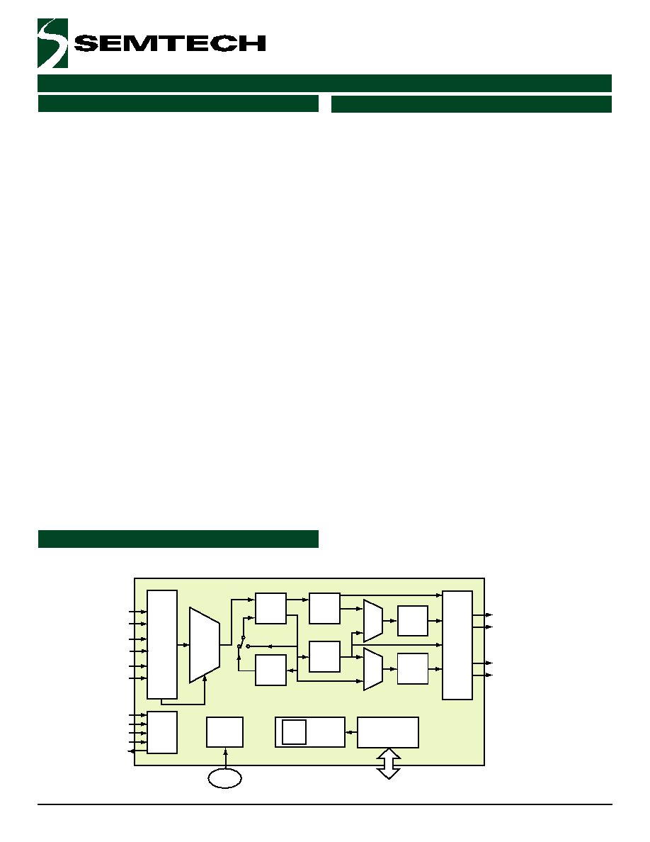
Figure 1 Block Diagram of the ACS8525 LC/P
Block Diagram
Description
Features
IEEE
1149.1
JTAG
Chip
Clock
Generator
TCK
TDI
TMS
TRST
TDO
F8525D_001BLOCKDIA_05
Selector
DPLL1
DPLL2
E1/DS1
Synthesis
APLL2
APLL3
APLL 1
01 and 02:
E1/DS1 (2.048/1.544 MHz)
and frequency multiples:
1.5x, 2x, 3x, 4x, 6x, 12x,
16x, and 24x E1/DS1
E3/DS3, 2 kHz, 8 kHz.
and OC-N* rates: OC-1 51.84 MHz
OC-3 155.52 MHz and derivatives:
6.48 MHz (O2 port only)
19.44 MHz, 25.92 MHz,
38.88 MHz, 51.84 MHz, 77.76 MHz,
155.52 MHz (01 port only)
311.04 MHz (01 port only)
3 x SEC/Sync Input Groups
SEC1 & SEC2:
TTL/PECL/LVDS,
SEC3 and all Syncs
TTL only
SEC Inputs:
Programmable
Frequencies
2 kHz, 4 kHz,
N x 8 kHz
1.544/2.048 MHz
6.48 MHz
19.44 MHz
25.92 MHz
38.88 MHz
51.84 MHz
77.76 MHz
155.52 MHz
FrSync 8 kHz (TTL)
Output
Port
Frequency
Selection
Priority
Table
Register Set
Digital Feedback
Serial Interface
Port
TCXO or
XO
Input
SEC Port
Monitors
and
Input
Selection
Control
Master
Slave
Stand-by
01 (PECL/LVDS)
02 (TTL)
MFrSync 2 kHz (TTL)
SEC Outputs:
Sync Outputs:
SEC1
SYNC1
SEC2
SYNC2
SEC3
SYNC3
MUX
2
MUX
1

Table of Contents
Revision 3.00/October 2003 © Semtech Corp.
Page 2
www.semtech.com
ACS8525 LC/P
Section
Page
ADVANCED COMMUNICATIONS
FINAL
DATASHEET
Description................................................................................................................................................................................................. 1
Block Diagram............................................................................................................................................................................................ 1
Features ..................................................................................................................................................................................................... 1
Table of Contents ...................................................................................................................................................................................... 2
Pin Diagram ............................................................................................................................................................................................... 4
Pin Description........................................................................................................................................................................................... 5
Introduction................................................................................................................................................................................................ 7
General Description................................................................................................................................................................................... 7
Inputs..................................................................................................................................................................................................7
Preconfiguring Inputs............................................................................................................................................................... 8
PECL/LVDS Input Port Selection ............................................................................................................................................. 9
Input Locking Frequency Modes ............................................................................................................................................. 9
Input SEC Activity Monitors ...............................................................................................................................................................9
Leaky Bucket Accumulator ................................................................................................................................................... 10
Fast Activity Monitor.............................................................................................................................................................. 11
Selector............................................................................................................................................................................................ 11
Selection of Input SECs......................................................................................................................................................... 11
External Protection Switching Mode-SRCSW pin ................................................................................................................ 13
Output Clock Phase Continuity on Source Switchover ....................................................................................................... 13
Forcing of the Operating Mode of the Device...................................................................................................................... 13
Phase Locked Loops (PLLs) ........................................................................................................................................................... 13
PLL Overview ......................................................................................................................................................................... 13
PLL Architecture .................................................................................................................................................................... 14
PLL Operational Controls ...................................................................................................................................................... 17
Phase Compensation Functions .......................................................................................................................................... 19
DPLL Feature Summary ........................................................................................................................................................ 20
Outputs ............................................................................................................................................................................................ 22
PECL/LVDS Output Port Selection ....................................................................................................................................... 22
Output Frequency Selection and PLL Configuration ........................................................................................................... 22
Operating Modes (States) of the Device ....................................................................................................................................... 30
Free-run Mode ....................................................................................................................................................................... 30
Pre-locked Mode ................................................................................................................................................................... 30
Locked Mode ......................................................................................................................................................................... 30
Lost-phase Mode................................................................................................................................................................... 30
Digital Holdover Mode........................................................................................................................................................... 30
Pre-locked2 Mode ................................................................................................................................................................. 32
Local Oscillator Clock...................................................................................................................................................................... 32
Status Reporting and Phase Measurement.................................................................................................................................. 32
Input Status Interrupts.......................................................................................................................................................... 32
Input Status Information....................................................................................................................................................... 32
DPLL Frequency Reporting ................................................................................................................................................... 32
Measuring Phase Between Master and Slave/Stand-by SEC Sources ............................................................................. 33
Sync Reference Sources ................................................................................................................................................................ 33
Aligning Phase of MFrSync and FrSync Outputs to Phase of Sync Inputs......................................................................... 34
Power-On Reset............................................................................................................................................................................... 35
Serial Interface................................................................................................................................................................................ 35
Register Map........................................................................................................................................................................................... 38
Register Organization ..................................................................................................................................................................... 38
Multi-word Registers ............................................................................................................................................................. 38
Register Access ..................................................................................................................................................................... 38
Interrupt Enable and Clear ................................................................................................................................................... 38
Defaults.................................................................................................................................................................................. 38
Register Descriptions ............................................................................................................................................................................. 42
Table of Contents

Revision 3.00/October 2003 © Semtech Corp.
Page 3
www.semtech.com
ACS8525 LC/P
Section
Page
ADVANCED COMMUNICATIONS
FINAL
DATASHEET
Electrical Specifications ......................................................................................................................................................................... 98
JTAG ................................................................................................................................................................................................. 98
Over-voltage Protection .................................................................................................................................................................. 98
ESD Protection ................................................................................................................................................................................ 98
Latchup Protection.......................................................................................................................................................................... 98
Maximum Ratings ........................................................................................................................................................................... 99
Operating Conditions ...................................................................................................................................................................... 99
DC Characteristics .......................................................................................................................................................................... 99
Jitter Performance ........................................................................................................................................................................103
Input/Output Timing .....................................................................................................................................................................105
Package Information ............................................................................................................................................................................ 106
Thermal Conditions.......................................................................................................................................................................107
Application Information........................................................................................................................................................................ 108
References............................................................................................................................................................................................ 109
Abbreviations ........................................................................................................................................................................................ 109
Notes ..................................................................................................................................................................................................... 110
Trademark Acknowledgements ........................................................................................................................................................... 110
Revision Status/History ....................................................................................................................................................................... 111
Ordering Information ............................................................................................................................................................................ 112
Disclaimers....................................................................................................................................................................................112
Contacts.........................................................................................................................................................................................112
ADVANCED COMMUNICATIONS
FINAL
DATASHEET
Revision 3.00/October 2003 © Semtech Corp.
Page 5
www.semtech.com
ACS8525 LC/P
Note...I = Input, O = Output, P = Power, TTL
U
= TTL input with pull-up resistor, TTL
D
= TTL input with pull-down resistor.
Pin Description
Table 1 Power Pins
Pin Number
Symbol
I/O
Type
Description
8, 9,
12
VD1+, VD2+,
VD3+
P
-
Supply Voltage: Digital supply to gates in analog section, +3.3 Volts
±10%.
22
VDD_DIFF
P
-
Supply Voltage: Digital supply for differential output pins 19 and 20,
+3.3 Volts ±10%.
27
VDD5V
P
-
Digital Supply for +5 Volts Tolerance to Input Pins. Connect to +5 Volts
(±10%) for clamping to +5 Volts. Connect to VDD for clamping to
+3.3 Volts. Leave floating for no clamping. Input pins tolerant up to
+5.5 Volts.
32, 36,
38, 39,
45, 46,
54
VDD1, VDD2,
VDD3, VDD4,
VDD5, VDD6,
VDD7
P
-
Supply Voltage: Digital supply to logic, +3.3 Volts ±10%.
4
VA1+
P
-
Supply Voltage: Analog supply to clock multiplying PLL,
+3.3 Volts ±10%.
14, 57
VA2+, VA3+
P
-
Supply Voltage: Analog supply to output PLLs APLL2 and APPL1,
+3.3 Volts ±10%.
15, 58
AGND3, AGND4
-
Supply Ground: Analog ground for output PLLs APLL2 and APPL1.
7, 10,
11
DGND1, DGND2,
DGND3
P
-
Supply Ground: Digital ground for components in PLLs.
31, 40,
53
DGND4, DGND5,
DGND6
P
-
Supply Ground: Digital ground for logic.
21
GND_DIFF
P
-
Supply Ground: Digital ground for differential ports.
1, 3
AGND1, AGND2
P
-
Supply Ground: Analog grounds.
Table 2 Internally Connected
Pin Number
Symbol
I/O
Type
Description
2, 16, 60, 61,
62, 63
IC1, IC2, IC3, IC4,
IC5, IC6,
-
-
Internally Connected: Leave to float.
55, 59
NC1, NC2
-
-
Not Connected: Leave to float.
Table 3 Other Pins
Pin Number
Symbol
I/O
Type
Description
5
INTREQ
O
TTL/CMOS
Interrupt Request: Active High/Low software Interrupt output.
6
REFCLK
I
TTL
Reference Clock: 12.800 MHz (refer to section headed Local Oscillator
Clock).
13
SRCSW
I
TTL
D
Source Switching: Force Fast Source Switching on SEC1 and SEC2.