 | –≠–ª–µ–∫—Ç—Ä–æ–Ω–Ω—ã–π –∫–æ–º–ø–æ–Ω–µ–Ω—Ç: E142AHF | –°–∫–∞—á–∞—Ç—å:  PDF PDF  ZIP ZIP |
EDGE HIGH-PERFORMANCE PRODUCTS
1
www.semtech.com
Edge142
Per Pin timing Deskew w 4x2
Cross Point Switch
Description
Features
Functional Block Diagram
Applications
Revision 1, February 14, 2000
The Edge142 is a 4 X 2 cross point switch with output
edge deskew capability. Manufactured in a high
performance bipolar process, it is designed primarily for
channel deskew applications in VLSI and Mixed-Signal
test equipment.
Any of the four input signals may be selected as the
source for either output. The 142 performs test head
multiplexing, adjacent channel multiplexing, and signal
buffering for both the drive and receive signals, in addition
to timing deskew.
The delay value (and resolution) is controlled via an
external voltage DAC. The delay element is designed
specifically to be monotonic and very stable while
delaying a very narrow pulse over a limited delay range.
The part offers separate delays for rising vs. falling edges.
The rising edge delay range is 1.5 ns and the falling
edge adjustment range is 300 ps.
The Edge142 is also well suited for 1:2 or 1:4 signal
fanout applications that require:
- multiple signal sources
- output enable / disable
- timing deskew on the output
signals.
∑ Very Narrow (<1 ns) Pulse Width Capability
∑ Fmax > 850 MHz
∑ Independent Delay Adjustments for Positive and
Negative Transitions
∑ Delay Range of 1.5 ns
∑ Trailing Edge Adjust Range of 300 ps
∑ Small Footprint: 52-pin MQFP Package
(10 X 10 mm) with Internal Heat Spreader or
Die Form
∑ Automatic Test Equipment
≠ Per pin deskew in VLSI, Mixed-Signal, and Memory
Testers
≠ Clock Distribution with timing adjustment
IN0 / 0*
IN1 / 1*
IN2 / 2*
IN3 / 3*
VDELAY 0
VFALL 0
OUT0 / 0*
OUT1 / 1*
MUX OUT0 / 0*
MUX OUT1 / 1*
VDELAY 1
VFALL 1
4 X 2
2 X 2
T
T

2
2000 Semtech Corp.
www.semtech.com
EDGE HIGH-PERFORMANCE PRODUCTS
Edge142
PIN Description
Pin Name
Pin #
Description
Digital
IN0, IN0*
IN1, IN1*
IN2, IN2*
IN3, IN3*
41, 42
44, 45
48, 47
51, 50
The multiplexer input signals. (Differential digital inputs.)
OUT0, OUT*
OUT1, OUT1*
26, 25
14, 15
The selected and delayed output signals. (Differential ECL compatible
outputs.)
MUX OUT0, 0*
MUX OUT1, 1*
23, 22
17, 18
Selected monitor outputs. (Differential ECL compatible levels.)
S00, S01
S10, S11
32, 31
8, 9
Single-ended 10KH ECL compatible inputs which select the channel 0
and channel 1 source.
MUX0 SEL
MUX1 SEL
30
10
Single-ended 10KH ECL compatible inputs which select the two output
monitor sources.
EN*
29
Single-ended 10KH ECL compatible input which enables the delayed
outputs.
MUX EN
11
Single-ended 10KH ECL compatible input which enables the monitor
outputs.
Analog
VDELAY0
VDELAY1
39
1
Analog voltage inputs which control the amount of propagation delay for
each channel.
VFALL0
VFALL1
37
3
Analog voltage inputs which control the amount of falling edge delay for
each channel.
VMID0
VMID1
38
2
Analog voltage inputs which control the amount of pulse width
compensation for each channel.
REXT1
36
Analog input current used to establish the bias current for the VDELAY,
VFALL, and VMIDinputs.
REXT2
4
Analog input current used to establish the bias level for the delay cells.
COMP1,
COMP2
35
5
Op Amp compensation capacitors.
TDP, TDN
21, 19
Positive and negative terminals to the thermal diode string.
Power
GND
6, 12, 13, 16,
24, 27, 28, 34,
40, 43, 49, 52
Device ground (positive device supply).
VEE
7, 20, 33, 46
3
2000 Semtech Corp.
www.semtech.com
EDGE HIGH-PERFORMANCE PRODUCTS
Edge142
PIN Description (continued)
VDELA
Y0
VMID0
VF
ALL0
REXT1
COMP1
GND
VEE
S00
S01
MUX0 SEL
EN*
GND
GND
GND
IN0
IN0*
GND
IN1
IN1*
VEE
IN2*
IN2
GND
IN3*
IN3
GND
OUT0
OUT0*
GND
MUX OUT0
MUX PUT0*
TDP
VEE
TDN
MUX OUT1*
MUX OUT1
GND
OUT1*
OUT1
VDELA
Y1
VMID1
VF
ALL1
REXT2
COMP2
GND
VEE
S10
S1
1
MUX1 SEL
MUX EN
GND
GND
1
2
3
4
5
6
7
8
9
10
11
12
13
39
38
37
26
35
34
33
32
31
30
29
28
27
26
25
24
23
22
21
20
19
18
17
16
15
14
40
41
42
43
44
45
46
47
48
49
50
51
52
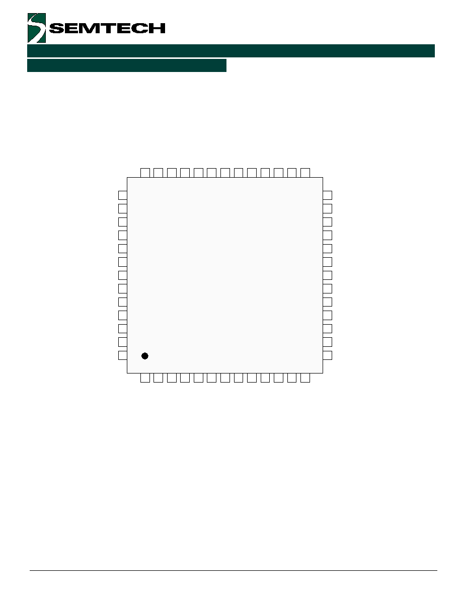
52-Pin MQFP 10mm x 10mm
with Internal Heat Spreader

4
2000 Semtech Corp.
www.semtech.com
EDGE HIGH-PERFORMANCE PRODUCTS
Edge142
Circuit Description
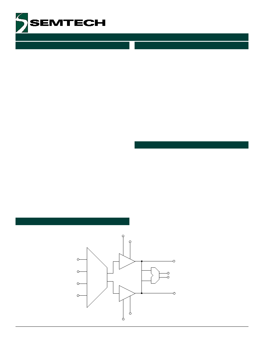
Chip Overview
The Edge142 is a 4 X 2 cross point switch and deskew
element, offering an 1.5 ns delay (Tspan), where the
VDELAY inputs adjust the overall propagation delay of
the part. In addition, the part supports a separate falling
edge delay of 300 ps (Tfall), where the VFALL inputs
control the falling edge delay.
Two additional outputs, which are selectable from either
OUT0 or OUT1, are provided. These outputs are useful
when attempting to fanout a selected input to multiple
destination without using and external buffer. All output
signals may be enabled or disabled.
The Edge142 is designed to be monotonic and very
stable. Figure 1 shows a simplified block diagram.
Figure 1. Edge142 Block Diagram
VDELAY0
VFALL0
OUT0 / 0*
OUT1 / 1*
MUX OUT0 / 0*
MUX OUT1 / 1*
VDELAY1
VFALL1
IN0 / 0*
IN1 / 1*
IN2 / 2*
IN3 / 3*
0
1
2
3
3
2
1
0
T
T
T
T
VMID1
MUX1 SEL
S11 S10
0
0
1
1
S01 S00
VMID0
MUX0 SEL EN* MUX EN
5
2000 Semtech Corp.
www.semtech.com
EDGE HIGH-PERFORMANCE PRODUCTS
Edge142
Circuit Description (continued)
Input Multiplexer
The Edge142 offers a 4 X 2 cross point switch in which
one of four input signals are selected to two independent
outputs. Each output signal's propagation delay and
pulse width may then be adjusted via external control.
The truth table below documents the multiplexer
functionality. Notice that there are no restrictions
between the selection of channel 0 and channel 1.
Output Multiplexer
The Edge142 provides MUX OUT0 / MUX OUT0* and
MUX OUT1 / MUX OUT1*, additional buffered differential
output signals. These signals are selected from OUT0
or OUT1, depending on the state of MUX SEL, as indicated
in the table below.
The MUX OUT signals allow either of the delayed outputs
to be sent to an alternative destination without having
to daisy chain the outputs to multiple destinations. This
feature permits point to point routing of all critical timing
signals in an effort to maintain the cleanest transmission
lines for these signals.
The MUX OUT signals also provide a method for sending
one common selected input signal to two independent
destinations. This feature is useful when fanning out
driver data and driver enable signals to multiple test
heads.
1
0
L
E
S
0
0
L
E
S
0
T
U
O
1
1
L
E
S
0
1
L
E
S
1
T
U
O
0
0
0
N
I
0
0
0
N
I
0
1
1
N
I
0
1
1
N
I
1
0
2
N
I
1
0
2
N
I
1
1
3
N
I
1
1
3
N
I
L
E
S
)
1
,
0
(
X
U
M
0
T
U
O
X
U
M
1
T
U
O
X
U
M
0
*
0
T
U
O
/
0
T
U
O
*
1
T
U
O
/
1
T
U
O
1
*
1
T
U
O
/
1
T
U
O
*
0
T
U
O
/
0
T
U
O
Output Enable
Both the output and multiplexer output signals may be
enabled or disabled, as documented below.
Propagation Delay Adjust
The Edge142 supports two independent delay functions,
which are described in the table below.
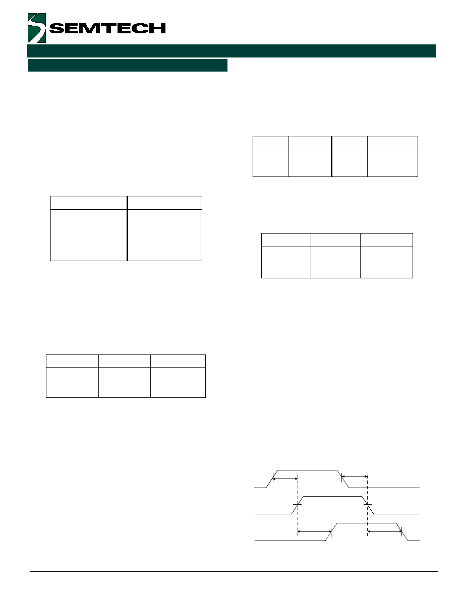
VDELAY controls the propagation delay of both the rising
and falling edge (see Figure 2). An input signal is
selected and then delayed by some programmable
amount (Tspan) determined by the analog input VDELAY.
The rising and falling edges are delayed equally. The
propagation delay for a rising and a falling edge is defined
as
Tpd+, Tpd- = Tpd(nom) + Tspan
where Tpd(nom) is the propagation delay of the part
with zero programmed delay, and Tspan is the additional
delay programmed via the VDELAY input. Notice that
Tspan can be either positive or negative, depending on
the nominal biasing of VDELAY, thus allowing bidirectional
propagation delay adjustment. The transfer function
for Tspan vs. VDELAY is shown in Figure 4.
*
N
E
*
T
U
O
/
T
U
O
N
E
X
U
M
T
U
O
)
1
,
0
(
X
U
M
0
e
v
i
t
c
A
0
0
1
0
1
e
v
i
t
c
A
+
d
p
T
-
d
p
T
Y
A
L
E
D
V
s
n
5
.
1
s
n
5
.
1
L
L
A
F
V
s
p
0
s
p
0
0
3
INPUT
OUTPUT
OUTPUT
(VDELAY = +0.1V)
(VDELAY = ≠1.3V)
TPD min
TPD min
Tspan
Tspan
Figure 2. VDELAY Control