 | –≠–ª–µ–∫—Ç—Ä–æ–Ω–Ω—ã–π –∫–æ–º–ø–æ–Ω–µ–Ω—Ç: E649 | –°–∫–∞—á–∞—Ç—å:  PDF PDF  ZIP ZIP |
EDGE HIGH-PERFORMANCE PRODUCTS
1
www.semtech.com
Edge649
Octal Pin Electronics
Driver/Receiver
Description
Features
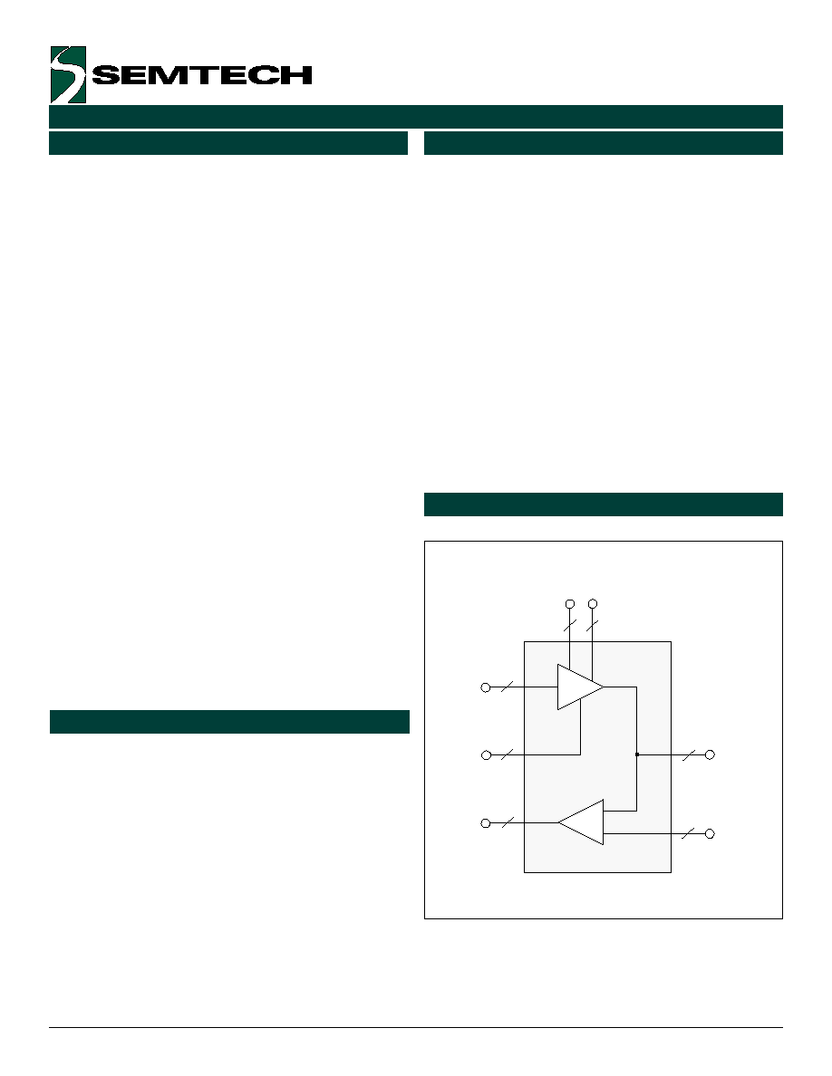
Functional Block Diagram
Applications
Revision 1/ October 28, 1996
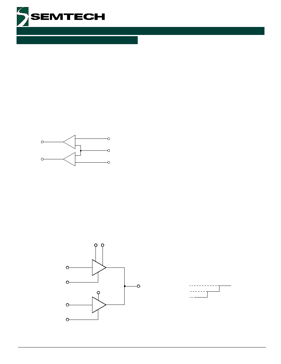
The Edge649 is an octal pin electronics driver and
receiver combination fabricated in a high- performance
CMOS process. It is designed for automatic test
equipment and instrumentation where cost, functional
density, and power are all at a premium.
The Edge649 incor porates eight channels of
programmable drivers and receivers into one package.
Each channel has per pin driver levels, receiver threshold,
and tristate control.
The 11V driver output and receiver input range allows
the Edge649 to interface directly between TTL, ECL,
CMOS (3V, 5V, and 8V), and custom level circuitry.
The Edge649 is pin and functionally compatible with the
EDGE648, with the following performance differences:
∑ reduced driver preshoot
∑ faster driver propagation delay
∑ superior driver pulse width distortion
∑ higher driver Fmax operation
∑ slightly slower driver output slew rates
∑ higher comparator Fmax operation
∑ lower comparator propagation delay
∑ superior comparator pulse width
distortion.
∑ 50 MHz Operation
∑ 11 V DUT I/O Range
∑ Programmable Output Levels
∑ Programmable Input Thresholds
∑ Per Pin Flexibility
∑ High Integration Levels
∑ 615 mW Quiescent Power Dissipation
∑ Edge648 Compatible
∑ Burn-In ATE
∑ Functional Board Testers
∑ In-Circuit Board Testers
∑ Combinational Board Testers
∑ Low Cost Chip Testers
∑ ASIC Verifiers
∑ VXI-Based Test Equipment
8
8
8
8
8
8
8
+
≠
VHIGH
VLOW
DUT
THRESHOLD
DATA IN
DVR EN*
DATA OUT

2
2000 Semtech Corp.
www.semtech.com
EDGE HIGH-PERFORMANCE PRODUCTS
Edge649
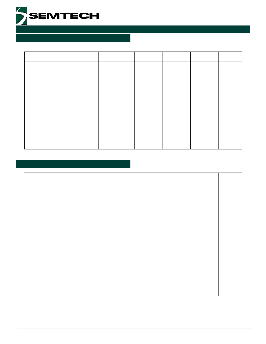
PIN Description
e
m
a
N
n
i
P
r
e
b
m
u
N
n
i
P
n
o
i
t
p
i
r
c
s
e
D
)
7
:
0
(
N
I
A
T
A
D
,
7
6
,
6
6
,
5
6
,
4
6
6
,
5
,
4
,
3
T
U
D
e
h
t
f
o
s
u
t
a
t
s
w
o
l
/
h
g
i
h
e
h
t
e
n
i
m
r
e
t
e
d
t
a
h
t
s
t
u
p
n
i
e
l
b
i
t
a
p
m
o
c
L
T
T
.
s
r
e
v
i
r
d
)
7
:
0
(
T
U
O
A
T
A
D
,
9
5
,
8
5
,
7
5
,
6
5
4
1
,
3
1
,
2
1
,
1
1
.
s
r
e
v
i
e
c
e
r
T
U
D
e
h
t
f
o
s
u
t
a
t
s
e
h
t
e
t
a
c
i
d
n
i
t
a
h
t
s
t
u
p
t
u
o
l
e
v
e
l
S
O
M
C
)
7
:
0
(
T
U
D
,
7
3
,
0
4
,
3
4
,
6
4
4
2
,
7
2
,
0
3
,
3
3
.
t
s
e
t
r
e
d
n
u
e
c
i
v
e
d
e
h
t
e
v
i
r
d
/
e
v
i
e
c
e
r
t
a
h
t
s
t
u
p
t
u
o
/
s
t
u
p
n
i
c
i
n
o
r
t
c
e
l
e
n
i
P
)
7
:
0
(
N
E
R
V
D
,
3
6
,
2
6
,
1
6
,
0
6
0
1
,
9
,
8
,
7
e
h
t
f
o
e
t
a
t
s
e
c
n
a
d
e
p
m
i
h
g
i
h
e
h
t
l
o
r
t
n
o
c
t
a
h
t
s
t
u
p
n
i
e
l
b
i
t
a
p
m
o
c
l
T
T
.
s
r
e
v
i
r
d
T
U
D
)
7
:
0
(
H
G
I
H
V
,
8
3
,
9
3
,
4
4
,
5
4
5
2
,
6
2
,
1
3
,
2
3
e
h
t
f
o
1
l
a
c
i
g
o
l
a
f
o
l
e
v
e
l
e
g
a
t
l
o
v
e
h
t
t
e
s
t
a
h
t
s
t
u
p
n
i
g
o
l
a
n
a
d
e
r
e
f
f
u
b
n
U
.
s
r
e
v
i
r
d
T
U
D
)
7
:
0
(
W
O
L
V
,
6
3
,
1
4
,
2
4
,
4
4
3
2
,
8
2
,
9
2
,
4
3
e
h
t
f
o
0
l
a
c
i
g
o
l
a
f
o
l
e
v
e
l
e
g
a
t
l
o
v
e
h
t
t
e
s
t
a
h
t
s
t
u
p
n
i
g
o
l
a
n
a
d
e
r
e
f
f
u
b
n
U
.
s
r
e
v
i
r
d
T
U
D
)
7
:
0
(
D
L
O
H
S
E
R
H
T
,
3
5
,
2
5
,
1
5
,
0
5
0
2
,
9
1
,
8
1
,
7
1
T
U
D
e
h
t
r
o
f
d
l
o
h
s
e
r
h
t
e
h
t
s
t
e
s
t
a
h
t
e
g
a
t
l
o
v
t
u
p
n
i
g
o
l
a
n
a
d
e
r
e
f
f
u
B
.
s
r
o
t
a
r
a
p
m
o
c
C
C
V
9
4
,
1
2
.
y
l
p
p
u
s
r
e
w
o
p
e
v
i
t
i
s
o
p
g
o
l
a
n
A
E
E
V
8
4
,
2
2
.
y
l
p
p
u
s
r
e
w
o
p
e
v
i
t
a
g
e
n
g
o
l
a
n
A
D
D
V
5
5
,
5
1
,
1
.
y
l
p
p
u
s
r
e
w
o
p
l
a
t
i
g
i
D
D
N
G
8
6
,
4
5
,
6
1
,
2
.
d
n
u
o
r
g
e
c
i
v
e
D
C
/
N
5
3
.
n
o
i
t
c
e
n
n
o
c
o
N
3
2000 Semtech Corp.
www.semtech.com
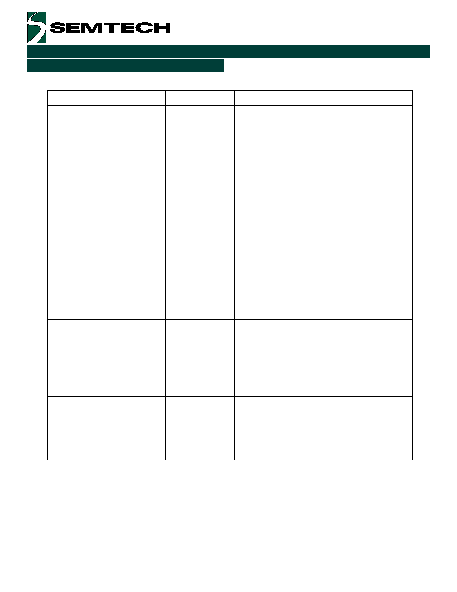
EDGE HIGH-PERFORMANCE PRODUCTS
Edge649
PIN Description (continued)
DVR EN*0
DA
T
A
OUT3
DA
T
A
OUT2
DA
T
A
OUT1
DA
T
A
OUT0
VDD
GND
THRESHOLD3
THRESHOLD2
THRESHOLD1
THRESHOLD0
VCC
VEE
VLOW0
DUT0
VHIGH0
VHIGH1
DUT1
VLOW1
VLOW2
DUT2
VHIGH2
VHIGH3
DUT3
VLOW3
NC
VLOW4
DUT4
VHIGH4
VHIGH5
DUT5
VLOW5
VLOW6
DUT6
DVR EN*1
DVR EN*2
DVR EN*3
DATA IN0
DATA IN1
DATA IN2
DATA IN3
GND
VDD
GND
DATA IN4
DATA IN5
DATA IN6
DATA IN7
DVR EN*4
DVR EN*5
DVR EN*6
DVR EN*7
DA
T
A
OUT4
DA
T
A
OUT5
DA
T
A
OUT6
DA
T
A
OUT7
VDD
GND
THRESHOLD4
THRESHOLD5
THRESHOLD6
THRESHOLD7
VCC
VEE
VLOW7
DUT7
VHIGH7
VHIGH6
60
59
58
57
56
55
54
53
52
51
50
49
48
47
46
45
44
10
11
12
13
14
15
16
17
18
19
20
21
22
23
24
25
26
61
62
63
64
65
66
67
68
1
2
3
4
5
6
7
8
9
43
42
41
40
39
38
37
36
35
34
33
32
31
30
29
28
27
4
2000 Semtech Corp.
www.semtech.com
EDGE HIGH-PERFORMANCE PRODUCTS
Edge649
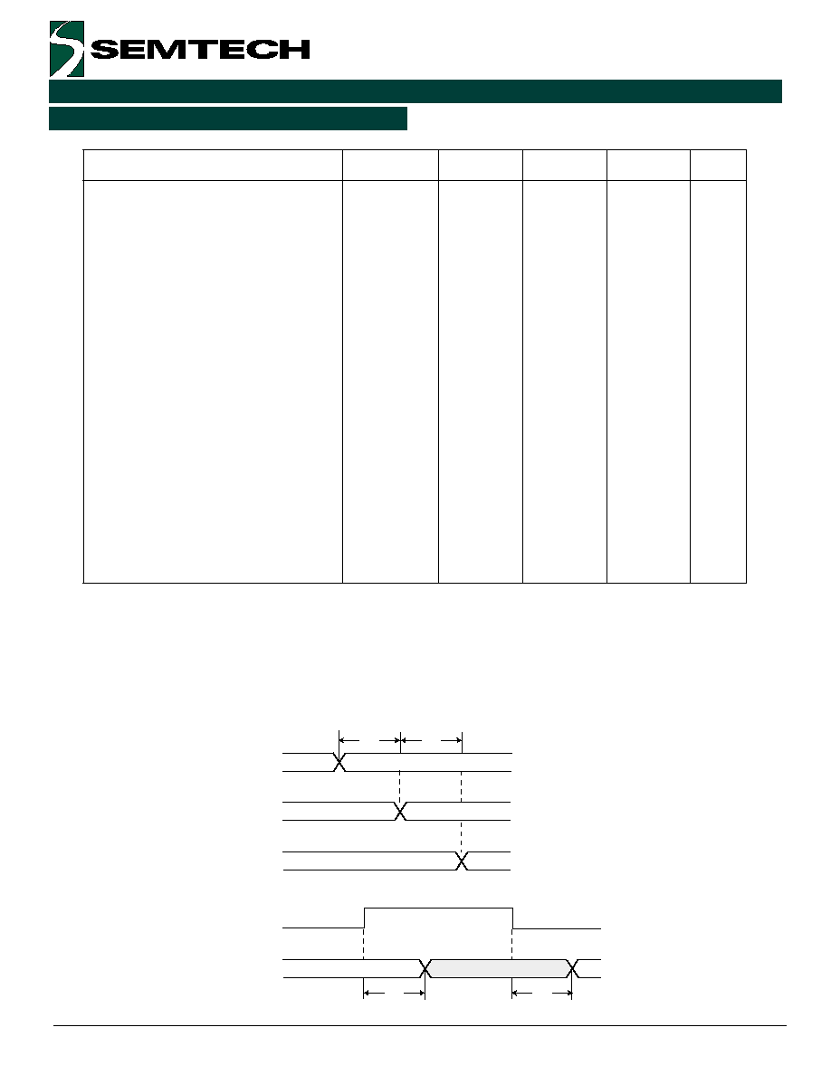
Circuit Description
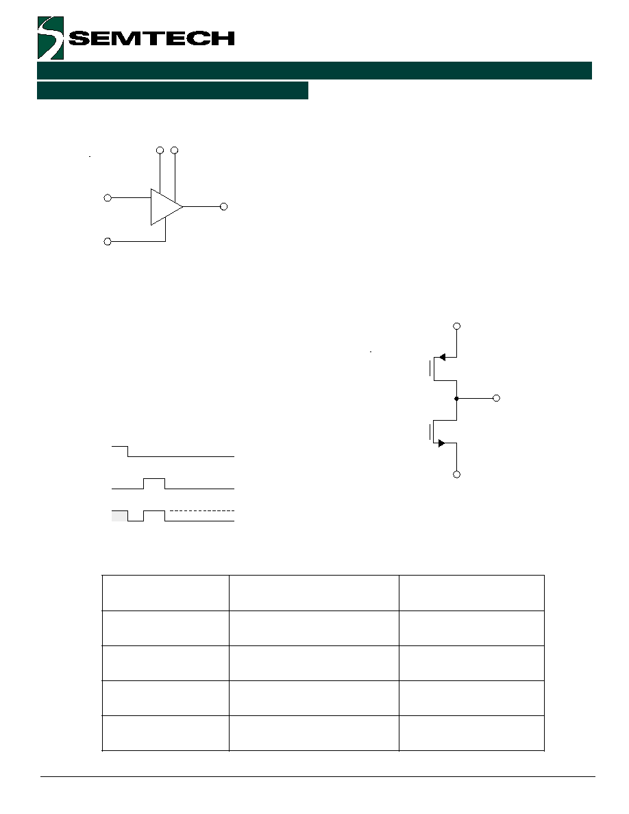
Driver Description
Figure 1. Driver Diagram
As shown in Figure 1, Edge649 supports programmable
high and low levels and tristate per channel. There are
no shared lines between any drivers. The DVR EN* and
DATA IN signals are TTL compatible inputs that control
the driver (see Figure 2).
With DVR EN* high, the DUT driver goes into a high
impedance state. With DVR EN* low, DATA IN high forces
the driver into a high state (DUT = V
HIGH
), and DATA IN
low forces the driver low (DUT = V
LOW
).
Figure 2. Driver Functionality
V
HIGH
and V
LOW
V
HIGH
and V
LOW
define the logical "1" and "0" levels of
the DUT driver and can be adjusted anywhere over the
range determined by VCC and VEE. Table 1 documents
the relationship between the analog power to supplies
(VCC and VEE), the driver range (V
HIGH
and V
LOW
), and
the comparator threshold range (V
THRESHOLD
).
The V
HIGH
and V
LOW
inputs are unbuffered in that they
also provide the driver output current (see Figure 3), so
the source of V
HIGH
and V
LOW
must have ample current
drive capability.
Figure 3.
Simplified Model of the
Unbuffered Output Stage
Table 1. Power Supply Requirement
e
v
i
e
c
e
R
/
e
v
i
r
D
e
g
n
a
R
e
d
o
M
n
o
m
m
o
C
d
l
o
h
s
e
r
h
T
e
g
n
a
R
y
l
p
p
u
S
r
e
w
o
P
s
n
o
i
t
i
d
n
o
C
V
5
.
6
+
=
<
T
U
D
=
<
V
0
V
0
.
5
=
<
D
L
O
H
S
E
R
H
T
=
<
V
1
.
0
V
5
.
6
+
=
C
C
V
V
0
=
E
E
V
V
8
+
=
<
T
U
D
=
<
V
0
V
5
.
6
=
<
D
L
O
H
S
E
R
H
T
=
<
V
1
.
0
V
8
+
=
C
C
V
V
0
=
E
E
V
V
1
1
+
=
<
T
U
D
=
<
V
0
V
5
.
9
=
<
D
L
O
H
S
E
R
H
T
=
<
V
1
.
0
V
1
1
+
C
C
V
V
0
=
E
E
V
V
8
+
=
<
T
U
D
=
<
V
3
-
V
5
.
6
=
<
D
L
O
H
S
E
R
H
T
=
<
V
9
.
2
-
V
8
+
=
C
C
V
V
3
-
=
E
E
V
VHIGH
VLOW
DUT
DATA IN
DVR EN*
VHIGH
VLOW
DUT
DATA IN
DVR EN*
VHIGH
VLOW
DUT
5
2000 Semtech Corp.
www.semtech.com
EDGE HIGH-PERFORMANCE PRODUCTS
Edge649
Circuit Description (continued)
Driver Output Protection
In a functional testing environment, where a resistor is
added in series with the driver output, the Edge649 can
withstand a short to any legal DUT voltage for an indefinite
amount of time.
In a low impedance application with no additional output
series resistance, care must be exercised and systems
should be designed to check for this condition and tristate
the driver if a short is detected.
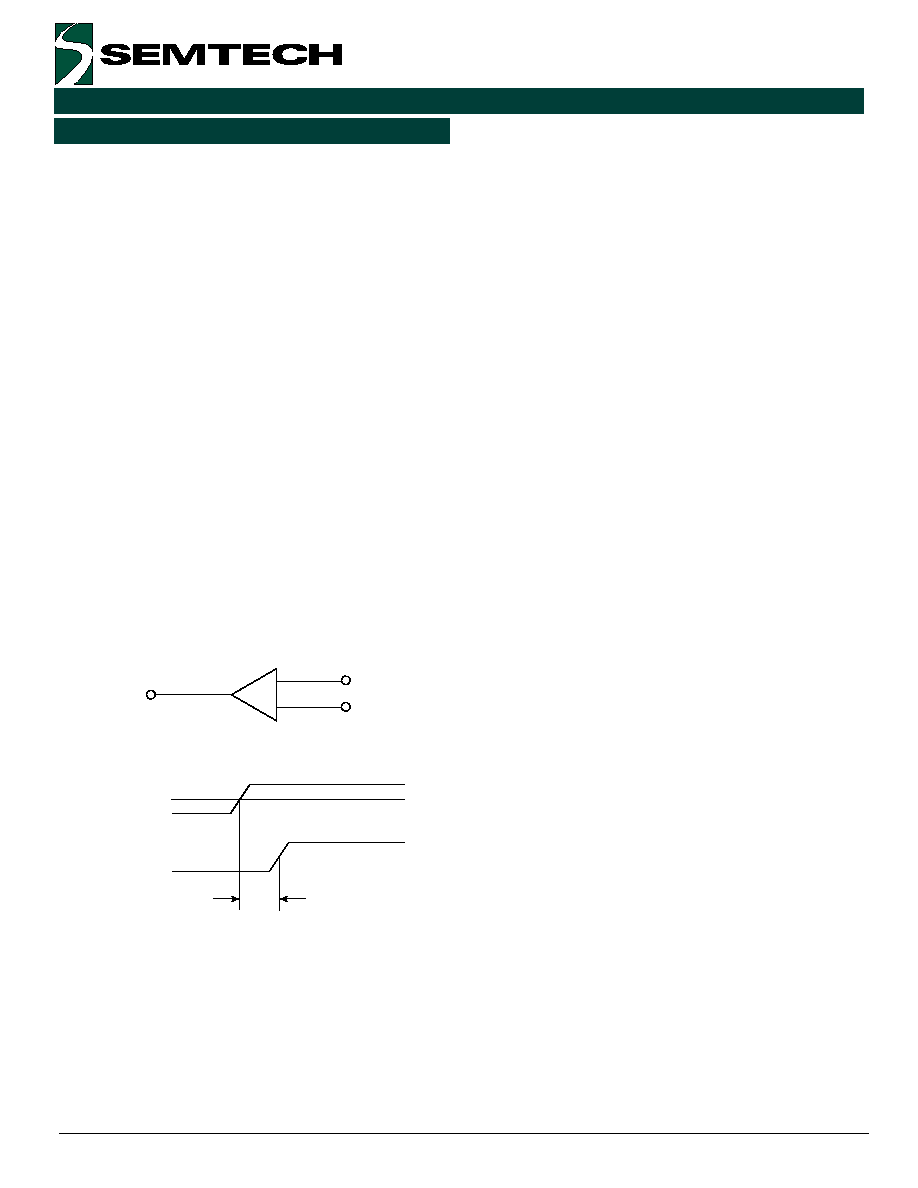
Receiver Functionality
Edge649 suppor ts programmable thresholds per
channel. There are no shared lines between comparators.
THRESHOLD is a high input impedance analog input
which defines a logical "1" and "0" at the DUT (see
Figure 4). If the DUT voltage is more positive than
THRESHOLD, DATA OUT will be high. With DUT lower
than THRESHOLD, DATA OUT will be low.
Figure 4. Receiver Functionality
DATA OUT
DUT
DUT
THRESHOLD
THRESHOLD
DATA OUT
Tpd
≠
+

6
2000 Semtech Corp.
www.semtech.com
EDGE HIGH-PERFORMANCE PRODUCTS
Edge649
Application Information
Power Supplies
The Edge649 uses three power supplies ≠ VDD, VCC
and VEE. VDD, typically +5V, is the digital supply for all
of the data inputs and outputs. VCC and VEE are the
analog power supplies for the DUT drivers and
comparators. VCC ranges from +6.5V to +11V, and must
be greater than or equal to VDD + 1.5V. VEE is the
negative analog power and typically varies from 0V to ≠
3V.
The Edge649 has several power supply requirements to
protect the part in power supply fault situations, as well
as during power up and power down sequences. VCC
must remain greater than or equal to VDD at all times.
Both VCC and VDD must always be positive (above
ground), and VEE must always be negative (at or below
ground).
The three-diode configuration shown in Figure 5, used
on a once-per-board basis, insures power supply
sequence and fault tolerance.
Figure 5.
Power Supply Protection Scheme
Power Supplies Decoupling
VDD, which provides the digital power, should be
decoupled to GND with a .1
µ
F chip capacitor in parallel
with a .001
µ
F chip capacitor. The bypass capacitors
should be as close to the device as possible. Power and
ground planes are recommended to provide a low
inductance return path.
VCC and VEE, which power the DUT drivers and receivers,
should also be decoupled to GND with a .1
µ
F chip
capacitor in parallel with a .001
µ
F chip capacitor. A
VCC and VEE plane, or at least a solid power bus, is
recommended for optimal performance.
V
HIGH
and V
LOW
Decoupling
As the V
HIGH
and V
LOW
inputs are unbuffered and must
supply the driver output current, decoupling capacitors
for these inputs are recommended in proportion to the
amount of output current the application requires
Expanding the Common Mode Range
Although the Edge649 can drive and receive 11V swings,
these 11 V signals can be adjusted over an 14V range.
By using programmable regulators V1 and V2 for the
VCC and VEE supplies (feasible because these two
analog power supplies do not supply driver output
current), the Edge649 I/O range can be optimized for a
variety of applications (see Figure 6).
Figure 6.
There are three rules which govern the supplies V1 and
V2:
1)
VDD + 1.5V
V1
+11V
2)
≠3V
V2
0V
3)
(V1 ≠ V2)
11V
VCC
VDD
VEE
1N5820 or
Equivalent
V1
Edge 649
V2
VCC
VDD
7
2000 Semtech Corp.
www.semtech.com
EDGE HIGH-PERFORMANCE PRODUCTS
Edge649
Application Information (continued)
Window Comparator
Certain applications require a dual threshold window
comparator to distinguish between the DUT being high,
low, or floating. To support this application, two Edge649
channels can be combined to create one channel with a
window comparator (see Figure 7). Notice that
connecting two DUT pins ties together the positive inputs
of both receivers. The result is a difference in polarity
between the digital outputs reporting the high and low
status of the DUT.
Figure 7. Edge649 as a
Window Comparator
Once two receivers are connected as window
comparators, the two drivers also get connected in
parallel. This dual driver configuration supports a
multitude of applications that have traditionally been
difficult to accommodate.
Trinary Driver
At times, there is a need for a three-level driver. Typically,
two levels are required for the standard digital "1" and
"0" pattern generation. The third level provides a higher
voltage to place the device under test (DUT) into a
programming or test mode. By controlling the DATA IN
and DVR EN* inputs, a trinary driver with tristate is
realizable (see Figure 8).
Driver with Pull Up/Pull Down
As the drivers are unbuffered, paralleling two drivers for
one DUT node provides a means for adding pull up or
pull down capability. By connecting the V
HIGH
and V
LOW
inputs of one driver through a resistor to a voltage,
additional functionality that would normally require an
external relay on the DUT transmission line to engage
and disengage these functions is realizable.
One common application for the pull up feature is testing
open collector devices. The pull down satisfies open
emitter DUTs (typically ECL). Either the pull up or down
could be used to establish a default high impedance
voltage on a bidirectional bus. Notice that in all
applications, the resistors can be switched dynamically
or statically.
Figure 8. Trinary Driver
DUT
High Threshold
Low Threshold
DUT LOW*
DUT HIGH
≠
+
≠
+
DUT
DATA IN A
DVR EN*A
DATA IN B
DVR EN*B
VHIGH A
VHIGH A
VHIGH B
VHIGH B
VLOW A
VLOW A
8
2000 Semtech Corp.
www.semtech.com
EDGE HIGH-PERFORMANCE PRODUCTS
Edge649
Application Information (continued)
Also, either the pull up or pull down resistor could be
used to terminate the transmission from the DUT to the
pin electronics in an effort to minimize any reflections.
Figure 9. Driver with Pull Up/Pull Down
Trinary Driver with Termination
Other combinations are also possible. For example, two
parallel drivers can be configured to implement one
trinary driver with a pull down (or pull up) dynamic
termination (see Figure 10).
Figure 10. Trinary Driver with Termination
Two Logic Family Driver
Many test systems support exactly two families of driver
and receiver levels and select between family A and family
B settings on a per-pin basis, typically using an analog
multiplexer, (See Figure 11.) Common examples of these
families are:
Family A = TTL
Family B = CMOS
or
Family A = TTL
Family B = ECL
The Edge649 supports this system architecture with
minimal hardware and the elimination of the per-pin
analog multiplexer. The drive and receive levels need to
be generated once per system, then distributed and
buffered suitably.
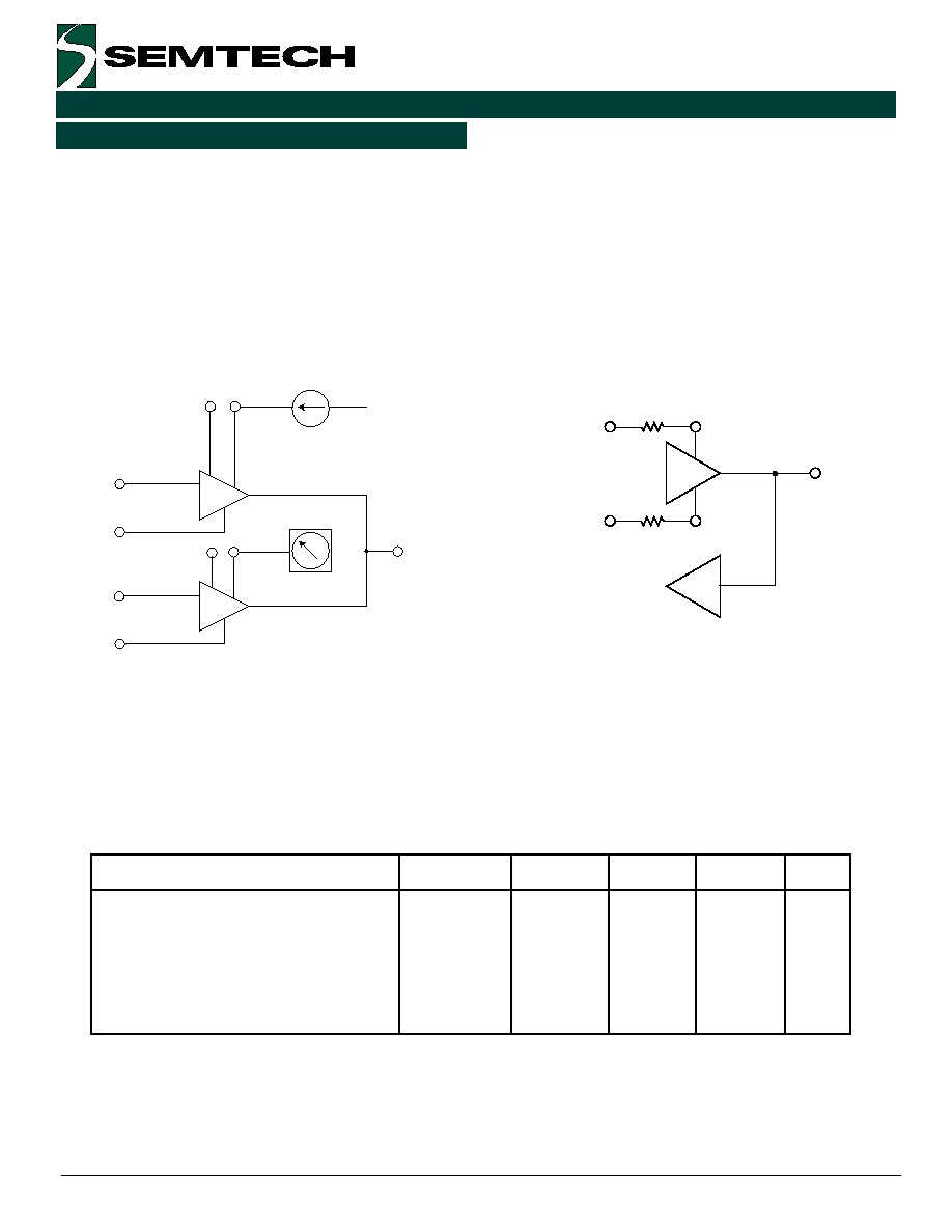
Parametric Functions
Two drivers in parallel also offer the possibility of
connecting force and sense parametric circuitry to the
DUT without adding additional circuitry to the controlled
impedance DUT line. For example, Figure 12 shows the
second driver being utilized to force a current and
measure a voltage.
Notice that the V
HIGH
and V
LOW
pins are used from
different drivers to allow the force and sense functions
to be active simultaneously.
DUT
DATA IN A
DVR EN*A
DATA IN B
DVR EN*B
VHIGH A
VHIGH B
VLOW B
VLOW A
VPULL UP
VPULL DOWN
DUT
DATA IN A
DVR EN*A
DATA IN B
DVR EN*B
VHIGH A
VHIGH B
VLOW A
VTERMINATION
Figure 11. Family A/B Using Two Drivers Per Pin
DUT0
DVR DATA
DVR EN*A
DVR EN*B
VHIGH A
VLOW B
VHIGH B
VLOW A
CHANNEL 1
DUT0
DVR DATA
DVR EN*A
DVR EN*B
CHANNEL n
9
2000 Semtech Corp.
www.semtech.com
EDGE HIGH-PERFORMANCE PRODUCTS
Edge649
Application Information (continued)
Figure 12. Edge649 Supporting Parametric Testing
Figure 13. Functional Application with
the Comparator Connected Directly to the DUT
Optional Output Configuration
Certain functional applications require a series output
resistor yet also demand that the comparator be
connected directly to the DUT, not via the backmatch
resistor. To create this configuration, two distinct
termination resistors may be connected to the V
HIGH
and V
LOW
input pins (see Figure 13).
VHIGH
DUT
DATA IN A
DATA EN* A
DATA IN B
DATA EN* B
PROGRAMMABLE
CURRENT
SOURCE
VLOW
VOLTAGE
MEASUREMENT
UNIT
DUT
VHIGH
VLOW
Thermal Information
r
e
t
e
m
a
r
a
P
l
o
b
m
y
S
n
i
M
p
y
T
x
a
M
s
t
i
n
U
e
c
n
a
t
s
i
s
e
R
l
a
m
r
e
h
T
e
s
a
C
o
t
n
o
i
t
c
n
u
J
C
J
8
.
9
o
W
/
C
r
i
A
o
t
n
o
i
t
c
n
u
J
r
i
A
l
l
i
t
S
M
P
F
L
0
5
M
P
F
L
0
0
4
A
J
A
J
A
J
4
3
6
2
9
1
o
W
/
C
o
W
/
C
o
W
/
C
10
2000 Semtech Corp.
www.semtech.com
EDGE HIGH-PERFORMANCE PRODUCTS
Edge649
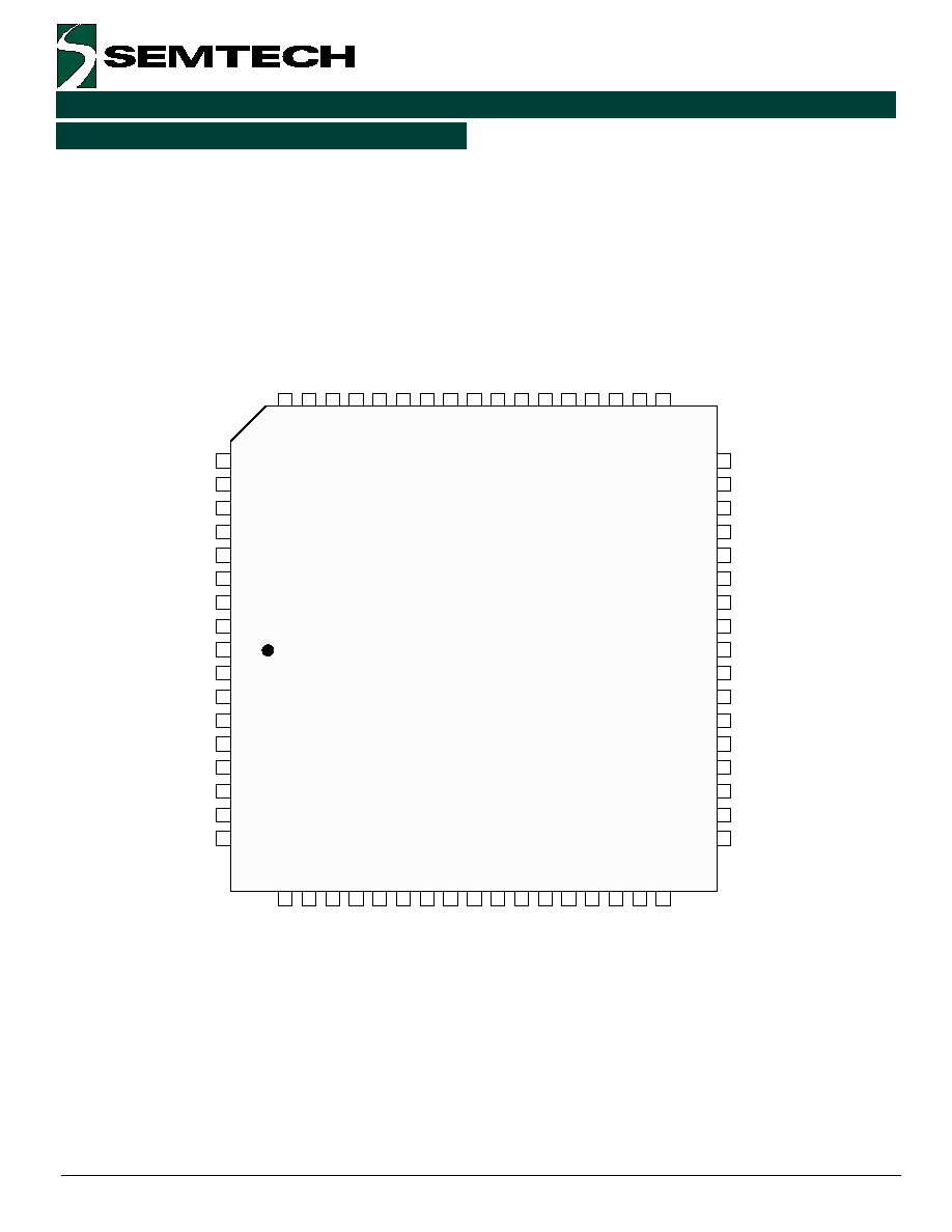
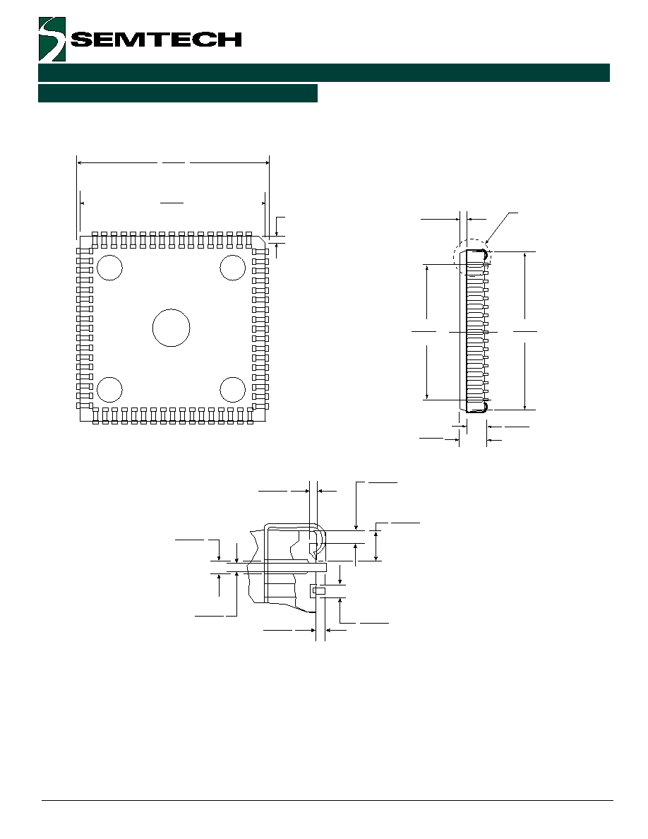
Package Information
PIN Descriptions
68 Pin PLCC Package
JA = 42 to 48∞C / W
Notes: (unless otherwise specified)
1.
Dimensions are in inches [millimeters].
2.
Tolerances are: .XXX
±
0.005 [0.127].
3.
PLCC packages are intended for surface mounting on solder lands on 0.050 [1.27] centers.
0.990 SQ
[25.146]
0.953 SQ
[24.206]
0.045 SQ
[1.143]
;
;
;
0.029
[0.736]
0.029
[0.736]
0.016
[0.406]
0.016
[0.406]
0.030
[0.762]
0.065
[1.651]
0.020
[0.508]
MIN
0.048
[1.219]
0.800 REF
[20.32]
0.910
[23.114]
See Detail A
0.175
[4.445]
0.113
[2.87]
11
2000 Semtech Corp.
www.semtech.com
EDGE HIGH-PERFORMANCE PRODUCTS
Edge649
Recommended Operating Conditions
Absolute Maximum Ratings
r
e
t
e
m
a
r
a
P
l
o
b
m
y
S
n
i
M
p
y
T
x
a
M
s
t
i
n
U
y
l
p
p
u
S
r
e
w
o
P
l
a
t
i
g
i
D
D
D
V
5
.
4
5
5
.
5
V
y
l
p
p
u
S
r
e
w
o
P
e
v
i
t
i
s
o
P
g
o
l
a
n
A
C
C
V
5
.
1
+
D
D
V
1
1
V
y
l
p
p
u
S
r
e
w
o
P
e
v
i
t
a
g
e
N
g
o
l
a
n
A
E
E
V
3
-
0
V
y
l
p
p
u
S
r
e
w
o
P
g
o
l
a
n
A
l
a
t
o
T
E
E
V
-
C
C
V
5
.
6
1
1
V
e
g
a
t
l
o
V
t
u
p
t
u
O
h
g
i
H
r
e
v
i
r
D
V
H
G
I
H
5
.
2
+
E
E
V
C
C
V
V
e
g
a
t
l
o
V
t
u
p
t
u
O
w
o
L
r
e
v
i
r
D
V
W
O
L
E
E
V
V
3
-
C
C
V
V
g
n
i
w
S
t
u
p
t
u
O
r
e
v
i
r
D
l
a
t
o
T
V
H
G
I
H
V
-
W
O
L
0
1
1
V
e
g
a
t
l
o
V
d
l
o
h
s
e
r
h
T
r
e
v
i
e
c
e
R
D
L
O
H
S
E
R
H
T
1
.
0
+
E
E
V
5
.
1
-
C
C
V
V
e
r
u
t
a
r
e
p
m
e
T
g
n
i
t
a
r
e
p
O
t
n
e
i
b
m
A
A
T
J
T
0
0
0
7
+
5
2
1
+
o
C
o
C
r
e
t
e
m
a
r
a
P
l
o
b
m
y
S
n
i
M
p
y
T
x
a
M
s
t
i
n
U
y
l
p
p
u
S
r
e
w
o
P
g
o
l
a
n
A
l
a
t
o
T
E
E
V
-
C
C
V
3
1
V
y
l
p
p
u
S
r
e
w
o
P
g
o
l
a
n
A
e
v
i
t
i
s
o
P
C
C
V
0
.
5
+
3
1
V
y
l
p
p
u
S
r
e
w
o
P
g
o
l
a
n
A
e
v
i
t
a
g
e
N
E
E
V
0
.
4
-
5
.
0
V
e
g
a
t
l
o
V
t
u
p
t
u
O
h
g
i
H
r
e
v
i
r
D
V
H
G
I
H
5
.
-
E
E
V
5
.
+
C
C
V
V
e
g
a
t
l
o
V
t
u
p
t
u
O
w
o
L
r
e
v
i
r
D
V
W
O
L
5
.
-
E
E
V
5
.
+
C
C
V
V
g
n
i
w
S
t
u
p
t
u
O
r
e
v
i
r
D
V
H
G
I
H
V
-
W
O
L
5
-
2
1
V
e
g
a
t
l
o
V
d
l
o
h
s
e
r
h
T
r
e
v
i
e
c
e
R
D
L
O
H
S
E
R
H
T
5
.
-
E
E
V
5
.
+
C
C
V
V
s
t
u
p
n
I
l
a
t
i
g
i
D
N
I
A
T
A
D
*
N
E
R
V
D
5
.
-
D
N
G
5
.
+
D
D
V
V
y
l
p
p
u
S
r
e
w
o
P
l
a
t
i
g
i
D
D
D
V
0
5
.
6
V
e
r
u
t
a
r
e
p
m
e
T
g
n
i
t
a
r
e
p
O
t
n
e
i
b
m
A
A
T
5
5
-
5
2
1
+
o
C
e
r
u
t
a
r
e
p
m
e
T
e
g
a
r
o
t
S
S
T
5
6
-
0
5
1
+
o
C
e
r
u
t
a
r
e
p
m
e
T
n
o
i
t
c
n
u
J
J
T
0
5
1
+
o
C
e
r
u
t
a
r
e
p
m
e
T
g
n
i
r
e
d
l
o
S
L
O
S
T
0
6
2
o
C
Stresses above those listed under "Absolute Maximum Ratings" may cause permanent damage to the
device. This is a stress rating only, and functional operation of the device at these, or any other conditions
beyond those listed, is not implied. Exposure to absolute maximum conditions for extended periods may
affect device reliability.
12
2000 Semtech Corp.
www.semtech.com
EDGE HIGH-PERFORMANCE PRODUCTS
Edge649
DC Characteristics
r
e
t
e
m
a
r
a
P
l
o
b
m
y
S
n
i
M
p
y
T
x
a
M
s
t
i
n
U
s
c
i
t
s
i
r
e
t
c
a
r
a
h
C
r
e
v
i
e
c
e
R
/
r
e
v
i
r
D
g
n
i
w
S
e
g
a
t
l
o
V
t
u
p
t
u
O
V
H
G
I
H
V
-
W
O
L
0
1
1
V
)
1
e
t
o
N
(
t
n
e
r
r
u
C
t
u
p
t
u
O
r
e
v
i
r
D
C
D
I
T
U
O
5
2
1
-
5
2
1
+
A
m
e
c
n
a
d
e
p
m
I
t
u
p
t
u
O
R
T
U
O
3
8
2
1
e
c
n
a
t
i
c
a
p
a
C
n
i
P
T
U
D
C
T
U
O
0
2
F
p
e
g
a
t
l
o
v
t
u
p
t
u
O
T
U
D
>
7
:
0
<
T
U
D
E
E
V
C
C
V
V
l
e
v
e
L
d
l
o
h
s
e
r
h
T
r
e
v
i
e
c
e
R
V
D
L
O
H
S
E
R
H
T
1
.
0
+
E
E
V
5
.
1
-
C
C
V
V
t
n
e
r
r
u
C
s
a
i
B
d
l
o
h
s
e
r
h
T
0
0
.
1
A
µ
t
n
e
r
r
u
C
t
u
p
n
I
e
g
a
k
a
e
L
T
U
D
I
S
A
I
B
2
0
0
.
0
.
1
A
µ
e
g
a
t
l
o
V
t
e
s
f
f
O
r
e
v
i
e
c
e
R
S
O
V
0
0
1
-
5
2
+
0
0
1
V
m
t
n
e
r
r
u
C
y
l
p
p
u
S
r
e
w
o
P
t
n
e
c
s
e
i
u
Q
y
l
p
p
u
S
r
e
w
o
P
e
v
i
t
i
s
o
P
y
l
p
p
u
S
r
e
w
o
P
e
v
i
t
a
g
e
N
y
l
p
p
u
S
r
e
w
o
P
l
a
t
i
g
i
D
C
C
I
E
E
I
D
D
I
5
2
5
2
0
2
0
4
0
4
5
3
A
m
A
m
A
m
m
o
o
r
d
a
e
H
r
e
v
i
r
D
E
E
V
o
t
h
g
i
H
r
e
v
i
r
D
C
C
V
o
t
w
o
L
r
e
v
i
r
D
V
H
G
I
H
V
-
E
E
V
-
C
C
V
W
O
L
5
.
2
0
.
3
V
V
s
t
u
p
n
I
l
a
t
i
g
i
D
)
7
:
0
(
*
N
E
R
V
D
,
)
7
:
0
(
N
I
A
T
A
D
e
g
a
t
l
o
V
h
g
i
H
t
u
p
n
I
H
I
V
N
I
M
0
.
2
V
e
g
a
t
l
o
V
w
o
L
t
u
p
n
I
L
I
V
X
A
M
8
.
0
V
t
n
e
r
r
u
C
t
u
p
n
I
I
N
I
0
.
1
A
µ
e
c
n
a
t
i
c
a
p
a
C
t
u
p
n
I
C
N
I
5
F
p
s
t
u
p
t
u
O
l
a
t
i
g
i
D
)
7
:
0
(
T
U
O
A
T
A
D
)
2
e
t
o
N
(
h
g
i
H
e
g
a
t
l
o
V
t
u
p
t
u
O
H
O
V
4
.
-
D
D
V
V
)
3
e
t
o
N
(
w
o
L
e
g
a
t
l
o
V
t
u
p
t
u
O
L
O
V
4
.
+
D
N
G
V
t
n
e
r
r
u
c
t
u
p
t
u
O
C
D
I
T
U
O
4
-
4
A
m
Note 1 :
Output current specification is per individual driver.
Note 2:
Output current of 4 mA.
Note 3:
Output current of ≠4 mA.
13
2000 Semtech Corp.
www.semtech.com
EDGE HIGH-PERFORMANCE PRODUCTS
Edge649
AC Characteristics
r
e
t
e
m
a
r
a
P
l
o
b
m
y
S
n
i
M
p
y
T
x
a
M
s
t
i
n
U
y
a
l
e
D
n
o
i
t
a
g
a
p
o
r
P
)
2
e
t
o
N
(
>
7
:
0
<
T
U
D
o
t
>
7
:
0
<
N
I
A
T
A
D
)
3
e
t
o
N
(
>
7
:
0
<
T
U
O
A
T
A
D
o
t
>
7
:
0
<
T
U
D
)
4
e
t
o
N
(
Z
i
H
o
t
e
v
i
t
c
A
)
4
e
t
o
N
(
e
v
i
t
c
A
o
t
Z
i
H
1
T
2
T
3
T
4
T
2
1
8
7
1
2
1
0
2
5
1
5
2
0
2
3
3
7
2
8
3
3
3
s
n
s
n
s
n
s
n
)
1
e
t
o
N
(
s
e
m
i
T
l
l
a
F
/
e
s
i
R
t
u
p
t
u
O
T
U
D
)
%
0
8
-
%
0
2
(
g
n
i
w
S
V
1
)
%
0
9
-
%
0
1
(
g
n
i
w
S
V
3
)
%
0
9
-
%
0
1
(
g
n
i
w
S
V
5
)
%
0
9
-
%
0
1
(
g
n
i
w
S
V
8
)
%
0
9
-
%
0
1
(
g
n
i
w
S
V
0
1
0
.
3
5
.
3
0
.
4
5
.
4
0
.
5
s
n
s
n
s
n
s
n
s
n
)
>
7
:
0
<
T
U
O
A
T
A
D
(
s
t
u
p
t
u
O
l
a
t
i
g
i
D
)
%
0
9
-
%
0
1
(
e
m
i
T
e
s
i
R
T
U
O
A
T
A
D
)
%
0
9
-
%
0
1
(
e
m
i
T
l
l
a
F
T
U
O
A
T
A
D
R
T
F
T
2
2
s
n
s
n
h
t
d
i
W
e
s
l
u
P
m
u
m
i
n
i
M
t
u
p
t
u
O
r
e
v
i
r
D
t
u
p
t
u
O
r
o
t
a
r
a
p
m
o
C
0
2
0
1
s
n
s
n
y
c
n
e
u
q
e
r
F
g
n
i
t
a
r
e
p
O
m
u
m
i
x
a
M
x
a
m
F
0
5
z
H
M
HiZ
T1
T2
T3
T4
DATA IN
DUT
DATA OUT
DVR EN*
DUT
Note 1:
Into 18 inches of 50
transmission line terminated with 1K
and 5 pF with the proper series
termination resistor.
Note 2:
Measured at 2.5V with a 10 mA load under the following conditions: VHIGH = +5.0V,
VLOW = 0V, VCC = +8V, VEE = -3V, and VDD = +5V.
Note 3:
Measured at 2.5V with a 4 mA load.
Note 4:
Load = 10 mA and measured when a 500 mV change at the output is detected.
14
2000 Semtech Corp.
www.semtech.com
EDGE HIGH-PERFORMANCE PRODUCTS
Edge649
Ordering Information
Contact Information
Semtech Corporation
Edge High-Performance Division
10021 Willow Creek Rd., San Diego, CA 92131
Phone: (858)695-1808 FAX (858)695-2633
r
e
b
m
u
N
l
e
d
o
M
e
g
a
k
c
a
P
J
P
B
9
4
6
E
C
C
L
P
n
i
P
-
8
6
M
V
E
9
4
6
M
V
E
e
l
u
d
o
M
n
o
i
t
a
u
l
a
v
E
9
4
6
e
g
d
E