 | –≠–ª–µ–∫—Ç—Ä–æ–Ω–Ω—ã–π –∫–æ–º–ø–æ–Ω–µ–Ω—Ç: E818AHF | –°–∫–∞—á–∞—Ç—å:  PDF PDF  ZIP ZIP |
EDGE HIGH-PERFORMANCE PRODUCTS
1
www.semtech.com
Edge818
Octal 18V Pin Electronics
Driver/window Comparator
Description
Features
Functional Block Diagram
Applications
Revision 1/ May 23, 2000
The Edge818 is an octal pin electronics driver and window
comparator fabricated in a wide voltage CMOS process.
It is designed specifically for Test During Burn In (TDBI)
applications, where cost, functional density, and power
are all at a premium.
The Edge818 incor porates eight channels of
programmable drivers and window comparators into one
14 mm X 20 mm 100 pin MQFP package. Each channel
has per pin driver levels, data, and high impedance
control. In addition, each comparator has per pin high
and low threshold levels.
The Edge818 uses "Flex In" and "Flex Out" digital inputs,
and can therefore mate directly with any digital technology
providing a minimum 2V swing. The digital outputs can
mate directly with any digital technology.
The 18V driver output and receiver input range allow the
Edge818 to interface directly with TTL, ECL, CMOS (3V,
5V, and 7V), LVCMOS, and custom level circuitry, as well
as the high voltage (Super Voltage) level required for
many special test modes for Flash Devices.
∑ 18V I/O Range
∑ 50 MHz Operation
∑ Per Pin Flexibility
∑ Programmable Input Thresholds
∑ Flex In Digital Inputs
∑ Flex Out Digital Outputs
∑ Small footprint (100 pin MQFP)
∑ Burn In ATE
∑ Low Cost ATE
∑ Instrumentation
8
8
8
8
8
8
8
8
DATA
EN*
QA
COMP HIGH
COMP LOW
QB
VH VL
DOUT
CVA
VINP
CVB
≠
+
+
≠
2
2000 Semtech Corp.
www.semtech.com
EDGE HIGH-PERFORMANCE PRODUCTS
Edge818
PIN Description
e
m
a
N
n
i
P
r
e
b
m
u
N
n
i
P
n
o
i
t
p
i
r
c
s
e
D
)
7
:
0
(
A
T
A
D
1
3
,
7
2
,
3
2
,
9
1
,
2
1
,
8
,
4
,
0
0
1
e
h
t
f
o
e
t
a
t
s
w
o
l
/
h
g
i
h
e
h
t
e
n
i
m
r
e
t
e
d
h
c
i
h
w
s
t
u
p
n
i
l
a
t
i
g
i
D
.
d
e
l
b
a
n
e
s
i
t
i
n
e
h
w
,
r
e
v
i
r
d
)
7
:
0
(
*
N
E
8
2
,
4
2
,
0
2
,
6
1
,
5
1
,
1
1
,
7
,
3
.
r
e
v
i
r
d
e
h
t
e
l
b
a
s
i
d
/
e
l
b
a
n
e
h
c
h
i
w
s
t
u
p
n
i
l
a
t
i
g
i
D
)
7
:
0
(
A
Q
)
7
:
0
(
B
Q
0
3
,
6
2
,
2
2
,
8
1
,
3
1
,
9
,
5
,
1
9
2
,
5
2
,
1
2
,
7
1
,
4
1
,
0
1
,
6
,
2
.
s
t
u
p
t
u
o
l
a
t
i
g
i
d
r
o
t
a
r
a
p
m
o
C
)
7
:
0
(
T
U
O
D
2
5
,
6
5
,
0
6
,
4
6
,
7
6
,
1
7
,
5
7
,
9
7
.
s
t
u
p
t
u
O
r
e
v
i
r
D
)
7
:
0
(
P
N
I
V
0
5
,
4
5
,
8
5
,
2
6
,
9
6
,
3
7
,
7
7
,
1
8
.
s
t
u
p
n
I
r
o
t
a
r
a
p
m
o
C
)
7
:
0
(
H
V
1
5
,
5
5
,
9
5
,
3
6
,
8
6
,
2
7
,
6
7
,
0
8
e
g
a
t
l
o
v
"
h
g
i
h
"
r
e
v
i
r
d
e
h
t
t
e
s
t
a
h
t
s
t
u
p
n
i
g
o
l
a
n
a
d
e
r
e
f
f
u
b
n
U
.
l
e
v
e
l
)
7
:
0
(
L
V
3
5
,
7
5
,
1
6
,
5
6
,
6
6
,
0
7
,
4
7
,
8
7
e
g
a
t
l
o
v
"
w
o
l
"
r
e
v
i
r
d
e
h
t
t
e
s
t
a
h
t
s
t
u
p
n
i
g
o
l
a
n
a
d
e
r
e
f
f
u
b
n
U
.
l
e
v
e
l
)
7
:
0
(
A
V
C
4
3
,
6
3
,
2
4
,
4
4
,
7
8
,
9
8
,
5
9
,
7
9
.
s
r
o
t
a
r
a
p
m
o
c
A
e
h
t
r
o
f
d
l
o
h
s
e
r
h
t
e
h
t
t
e
s
t
a
h
t
s
t
u
p
n
i
g
o
l
a
n
A
)
7
:
0
(
B
V
C
5
3
,
7
3
,
3
4
,
5
4
,
6
8
,
8
8
,
4
9
,
6
9
.
s
r
o
t
a
r
a
p
m
o
c
B
e
h
t
r
o
f
d
l
o
h
s
e
r
h
t
e
h
t
t
e
s
t
a
h
t
s
t
u
p
n
i
g
o
l
a
n
A
B
B
V
5
8
,
6
4
l
a
t
i
g
i
d
e
h
t
r
o
f
d
l
o
h
s
e
r
h
t
e
h
t
s
t
e
s
t
a
h
t
e
g
a
t
l
o
v
t
u
p
n
i
g
o
l
a
n
A
.
s
t
u
p
n
i
H
G
I
H
P
M
O
C
8
9
,
3
3
e
h
t
f
o
l
e
v
e
l
h
g
i
h
e
h
t
s
t
e
s
t
a
h
t
t
u
p
n
i
g
o
l
a
n
a
d
e
r
e
f
f
u
b
n
U
.
s
t
u
p
t
u
o
r
o
t
a
r
a
p
m
o
c
W
O
L
P
M
O
C
9
9
,
2
3
e
h
t
f
o
l
e
v
e
l
w
o
l
e
h
t
s
t
e
s
t
a
h
t
t
u
p
n
i
g
o
l
a
n
a
d
e
r
e
f
f
u
b
n
U
.
s
t
u
p
t
u
o
r
o
t
a
r
a
p
m
o
c
C
C
V
1
9
,
0
9
,
4
8
,
2
8
,
9
4
,
7
4
,
1
4
,
0
4
.
y
l
p
p
u
s
r
e
w
o
p
e
v
i
t
i
s
o
P
E
E
V
3
9
,
2
9
,
3
8
,
8
4
,
9
3
,
8
3
.
y
l
p
p
u
s
r
e
w
o
p
e
v
i
t
a
g
e
N
3
2000 Semtech Corp.
www.semtech.com
EDGE HIGH-PERFORMANCE PRODUCTS
Edge818
PIN Description (continued)
D
ATA
0
COMP
LOW
COMP
HIGH
CV
A0
CVB0
CV
A1
CVB1
VEE
VEE
VCC
VCC
CV
A2
CVB2
CV
A3
CVB3
VBB
VCC
VEE
VCC
VINP0
D
ATA
7
COMP
LOW
COMP
HIGH
CV
A7
CVB7
CV
A6
CVB6
VEE
VEE
VCC
VCC
CV
A5
CVB5
CV
A4
CVB4
VBB
VCC
VEE
VCC
VINP7
VH0
DOUT0
VL0
VINP1
VH1
DOUT1
VL1
VINP2
VH2
DOUT2
VL2
VINP3
VH3
DOUT3
VL3
VL4
DOUT4
VH4
VINP4
VL5
DOUT5
VH5
VINP5
VL6
DOUT6
VH6
VINP6
VL7
DOUT7
VH7
QA0
QB0
EN*0
DATA1
QA1
QB1
EN*1
DATA2
QA2
QB2
EN*2
DATA3
QA3
QB3
EN*3
EN*4
QB4
QA4
DATA4
EN*5
QB5
QA5
DATA5
EN*6
QB6
QA6
DATA6
EN*7
QB7
QA7
1
31
51
81
100 Lead - 14 x 20 MQFP
4
2000 Semtech Corp.
www.semtech.com
EDGE HIGH-PERFORMANCE PRODUCTS
Edge818
Circuit Description
Driver Description
The Edge818 supports programmable high and low levels
and tristate per channel. There are no shared lines
between any drivers. The EN* and DATA signals are
wide voltage high impedance analog inputs capable of
receiving digital signals over a wide common mode range.
VBB is the high impedance analog input which sets the
threshold for EN* and DATA.
EN*, DATA
Status
> VBB
"1"
< VBB
"0"
With EN* high, the driver goes into a high impedance
state. With EN* low, DATA high forces the driver into a
high state, and DATA low forces the driver into a low
state.
EN*
DATA
DOUT
1
X
HiZ
0
1
VH
0
0
VL
Drive High and Low
VH and VL define the logical "1" and "0" levels of the
driver, and can be adjusted anywhere over the range
determined by VCC and VEE. There are no restrictions
between VH and VL, other than they must remain within
the power supply levels.
VEE
VH
VCC
VEE
VL
VCC
The VH and VL inputs are unbuffered in that they also
provide the driver output current (see Figure 3), so the
source of VH and VL must have ample current drive
capability.
Figure 3. Simplified Model of the
Unbuffered Output Stage
Driver Output Protection
In a functional testing environment, where a resistor is
added in series with the driver output to create a 50
driver, the Edge818 can withstand a short to any legal
voltage for an indefinite amount of time.
In a low impedance application, with no additional output
resistance, the system should be designed to check for
a short circuit prior to connecting the driver, and tristate
the driver if a short is detected.
Receiver Description
The Edge818 suppor ts a window comparator with
independent threshold levels per channel. There are no
shared comparator lines between channels. CVA and
CVB are high impedance analog voltage inputs which
define the threshold voltages for comparators A and B.
If VINP is more positive than CVA or CVB, QA and QB will
be high. Otherwise, QA and QB will be low.
VINP
QA
VINP > CVA
COMP HIGH
VINP < CVA
COMP LOW
VINP
QB
VINP > CVB
COMP HIGH
VINP < CVB
COMP LOW
VH
VL
DUT
5
2000 Semtech Corp.
www.semtech.com
EDGE HIGH-PERFORMANCE PRODUCTS
Edge818
Circuit Description (continued)
The comparator outputs are "Flex Out". They are
technology independent and may be adjusted over a wide
voltage common mode range. COMP HIGH and COMP
LOW are analog inputs which set the digital high and low
levels (respectively) of QA and QB. COMP HIGH and
COMP LOW are unbuffered inputs that provide the
necessary drive current, so the sources for these levels
must have adequate current capability.
Figure 4. Simplified Model of the
Unbuffered Comparator Output Stage
Typically, COMP HIGH and COMP LOW will be connected
to the digital power supplies of the chip receiving QA
and QB.
Receiver Headroom
There is ~2V of headroom required between the
comparator thresholds and both power supply levels.
VEE + 2.0
CVA, CVB
VCC ≠ 2.0
COMP HIGH
COMP LOW
QAX, QBX
6
2000 Semtech Corp.
www.semtech.com
EDGE HIGH-PERFORMANCE PRODUCTS
Edge818
Application Information
Power Supply Decoupling
VCC and VEE should be decoupled to GND with a .1
µ
F
chip capacitor in parallel with a .001
µ
F chip capacitor.
A VCC and VEE plane, or at least a solid power bus, is
recommended for optimal performance.
VH and VL Decoupling
As the VH and VL inputs are unbuffered and supply the
driver output current, which can be quite large during
edge transitions, decoupling capacitors for these inputs
are recommended in proportion to the amount of output
current requirements.
For applications where VH and VL are shared over multiple
channels, a solid power plane to distribute these levels
is preferred.
VBB
The two VBB pins are connected together on-chip.
Therefore, only one VBB needs to be connected to for
proper 818 operation.
The two pins may be used to daisy chain a VBB signal
across a PC Board without having to route the actual
signal underneath the 818.
Latchup Protection
The Edge818 has several power supply requirements to
protect the part in power supply fault situations, as well
as during power up and power down sequences. VCC
must remain greater than or equal to VDD (external supply
for the digital logic) at all times. Both VCC and VDD
must always be positive (above ground), and VEE must
always be negative (at or below ground).
The three diode configuration shown in Figure 5 should
be used on a once-per-board basis.
Figure 5.
Power Supply Protection Scheme
gure 5.
Warning: It is extremely important that the voltage on
any device pin does not exceed the range of VEE ≠
0.5V to VCC +0.5V at any time, either during power up,
normal operation, or during power down. Failure to
adhere to this requirement could result in latchup of
the device, which could be destructive if the system
power supplies are capable of supplying large amounts
of current. Even if the device is not immediately
destroyed, the cumulative damage caused by the stress
of repeated latchup may affect device reliability.
VCC
VDD
VEE
1N5820 or
Equivalent
7
2000 Semtech Corp.
www.semtech.com
EDGE HIGH-PERFORMANCE PRODUCTS
Edge818
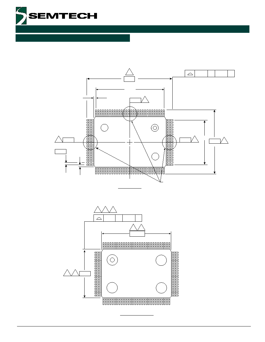
Package Information
PIN Descriptions
D2
E2
D
Z
D
Z
E
4
3
3
≠D≠
3
≠B≠
4
≠E≠
≠A≠
e
SEE DETAIL "A"
TOP VIEW
0.25
C
D
4X
A ≠ B
0.20
4X
C
D
A ≠ B
D1
2
5
7
5
7
5
7
E1
C
O O
BOTTOM VIEW
100-Pin MQFP
14 mm x 20 mm
8
2000 Semtech Corp.
www.semtech.com
EDGE HIGH-PERFORMANCE PRODUCTS
Edge818
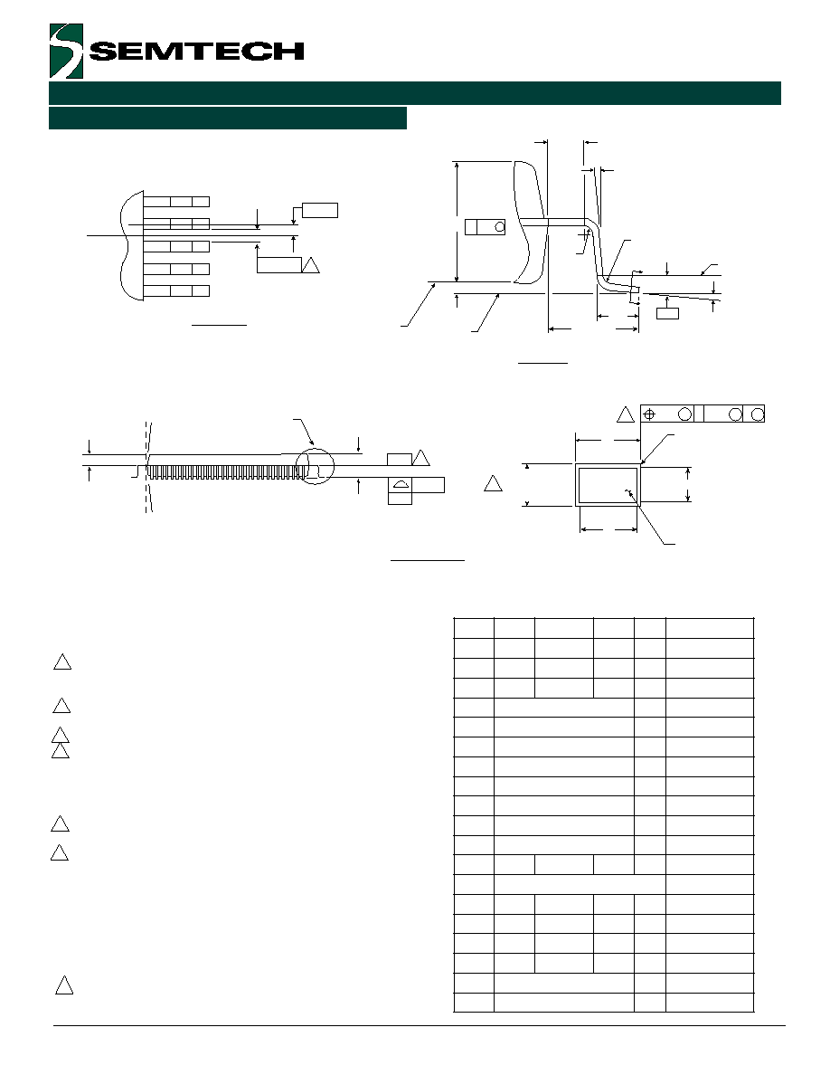
Package Information (continued)
≠A, B, D≠
3
e / 2
DETAIL "A"
≠
0.40 MIN.
0 ≠ 7
∞
∞
0.13 / 0.30 R. TYP.
GAGE
PLANE
BASE
PLANE
SEATING
PLANE
0.25
1.60 REF.
L
C
C
A2
0.10 S
0.13
R. MIN.
DETAIL "B"
0 MIN.
A1
≠H≠
0.076
≠C≠
2
8
12
B
12 ≠ 16
∞
12 ≠ 16
∞
D
C
S
M
S
ccc
A ≠ B
A
SEE DETAIL "B"
B
1
BASE METAL
0.13 / 0.17
0.13 / 0.23
1.28 REF.
WITH LEAD FINISH
SECTION C≠C
Notes:
1. All dimensions and tolerances conform to ANSI Y14.5-1982.
2. Datum plane -H- located at mold parting line and coincident
with lead, where lead exits plastic body at bottom of parting
line.
3. Datums A-B and -D- to be determined where centerline between
leads exits plastic body at datum plane -H-.
4. To be determined at seating plane -C-.
5. Dimensions D1 and E1 do not include mold protrusion.
Allowable mold protrusion is 0.254 mm per side. Dimensions
D1 and E1 do include mold mismatch and are determined at
datum plane -H-.
6. "N" is the total # of terminals.
7. Package top dimensions are smaller than bottom dimensions
and top of package will not overhang bottom of package.
8. Dimension B does not include dambar protrusion. Allowable
dambar protrusion shall be 0.08 mm total in excess of the
dimension at maximum material condition. Dambar cannot
be located on the lowerradius or the foot.
9. All dimensions are in millimeters.
10. Maximum allowable die thickness to be assembled in this
package family is 0.635 millimeters.
11. This drawing conforms to JEDEC registered outlines MS-108
and MS-022.
12. These dimensions apply to the flat section of the lead between
0.10 mm and 0.25 mm from the lead tip.
l
o
b
m
y
S
n
i
M
m
o
N
x
a
M
e
t
o
N
s
t
n
e
m
m
o
C
A
4
0
.
3
0
4
.
3
B
C
P
e
v
o
b
a
t
h
g
i
e
H
1
A
5
2
.
0
3
3
.
0
B
C
P
e
v
o
b
a
p
a
G
2
A
7
5
.
2
1
7
.
2
7
8
.
2
s
s
e
n
k
c
i
h
T
y
d
o
B
D
C
S
B
0
2
.
3
2
4
1
D
C
S
B
0
0
.
0
2
5
n
o
i
s
n
e
m
i
D
y
d
o
B
2
D
F
E
R
5
8
.
8
1
D
Z
F
E
R
8
5
.
0
E
0
2
.
7
1
4
1
E
C
S
B
0
0
.
4
1
5
n
o
i
s
n
e
m
i
D
y
d
o
B
2
E
F
E
R
5
3
.
2
1
E
Z
F
E
R
3
8
.
0
L
3
7
.
0
8
8
.
0
3
0
.
1
N
0
0
1
6
t
n
u
o
C
n
i
P
e
C
S
B
5
6
.
0
h
c
t
i
P
d
a
e
L
B
2
2
.
0
8
3
.
0
8
n
o
i
s
n
e
m
i
D
d
a
P
1
B
2
2
.
0
0
3
.
0
3
3
.
0
n
o
i
s
n
e
m
i
D
d
a
P
c
c
c
3
1
.
0
D
N
0
3
t
n
u
o
C
n
i
P
e
d
i
S
E
N
0
2
t
n
u
o
C
n
i
P
e
d
i
S
Variations
(all dimensions in millimeters)

9
2000 Semtech Corp.
www.semtech.com
EDGE HIGH-PERFORMANCE PRODUCTS
Edge818
Recommended Operating Conditions
Absolute Maximum Ratings
r
e
t
e
m
a
r
a
P
l
o
b
m
y
S
n
i
M
p
y
T
x
a
M
s
t
i
n
U
y
l
p
p
u
S
g
o
l
a
n
A
l
a
t
o
T
E
E
V
-
C
C
V
0
.
2
1
0
.
8
1
V
e
r
u
t
a
r
e
p
m
e
T
g
n
i
t
a
r
e
p
O
t
n
e
i
b
m
A
A
T
0
7
+
o
C
e
r
u
t
a
r
e
p
m
e
T
n
o
i
t
c
n
u
J
J
T
5
2
1
+
o
C
r
e
t
e
m
a
r
a
P
l
o
b
m
y
S
n
i
M
x
a
M
s
t
i
n
U
y
l
p
p
u
S
r
e
w
o
P
l
a
t
o
T
E
E
V
-
C
C
V
5
.
0
-
0
.
9
1
V
s
e
g
a
t
l
o
V
t
u
p
n
I
l
a
t
i
g
i
D
*
N
E
,
A
T
A
D
5
.
-
E
E
V
5
.
+
C
C
V
V
s
e
g
a
t
l
o
V
t
u
p
n
I
g
o
l
a
n
A
B
B
V
,
P
N
I
V
,
B
V
C
,
A
V
C
,
L
V
,
H
V
5
.
-
E
E
V
5
.
+
C
C
V
V
s
e
g
a
t
l
o
V
t
u
p
t
u
O
g
o
l
a
n
A
W
O
L
P
M
O
C
,
H
G
I
H
P
M
O
C
,
T
U
O
D
5
.
-
E
E
V
5
.
+
C
C
V
V
e
r
u
t
a
r
e
p
m
e
T
g
n
i
t
a
r
e
p
O
t
n
e
i
b
m
A
A
T
0
5
-
5
2
1
+
o
C
e
r
u
t
a
r
e
p
m
e
T
e
g
a
r
o
t
S
S
T
5
6
-
0
5
1
+
o
C
e
r
u
t
a
r
e
p
m
e
T
n
o
i
t
c
n
u
J
J
T
0
5
1
+
o
C
e
r
u
t
a
r
e
p
m
e
T
g
n
i
r
e
d
l
o
S
)
n
i
p
e
h
t
m
o
r
f
"
5
2
.
,
s
d
n
o
c
e
s
5
(
L
O
S
T
0
6
2
+
o
C
Stresses above those listed under "Absolute Maximum Ratings" may cause permanent damage to the
device. This is a stress rating only, and functional operation of the device at these, or any other conditions
beyond those listed, is not implied. Exposure to absolute maximum conditions for extended periods may
affect device reliability.
10
2000 Semtech Corp.
www.semtech.com
EDGE HIGH-PERFORMANCE PRODUCTS
Edge818
DC Characteristics
r
e
t
e
m
a
r
a
P
l
o
b
m
y
S
n
i
M
p
y
T
x
a
M
s
t
i
n
U
r
e
v
i
r
D
e
g
a
t
l
o
V
h
g
i
H
e
g
a
t
l
o
V
w
o
L
g
n
i
w
S
t
u
p
t
u
O
t
n
e
r
r
u
C
e
g
a
k
a
e
L
Z
i
H
e
c
n
a
d
e
p
m
I
t
u
p
t
u
O
)
1
e
t
o
N
(
t
n
e
r
r
u
C
t
u
p
t
u
O
C
D
)
2
e
t
o
N
(
t
n
e
r
r
u
C
t
u
p
t
u
O
C
A
H
V
L
V
L
V
-
H
V
k
a
e
l
I
t
u
o
R
C
D
t
u
o
I
C
A
t
u
o
I
E
E
V
E
E
V
E
E
V
0
.
2
-
0
.
9
5
2
1
-
0
0
4
-
0
2
1
C
C
V
C
C
V
C
C
V
0
.
2
+
5
1
5
2
1
+
0
0
4
+
V
V
V
A
n
A
m
A
m
r
e
v
i
e
c
e
R
e
g
n
a
R
e
g
a
t
l
o
V
t
u
p
n
I
e
g
n
a
R
e
g
a
t
l
o
V
d
l
o
h
s
e
r
h
T
)
3
e
t
o
N
(
e
g
a
t
l
o
V
t
e
s
f
f
O
t
n
e
r
r
u
C
s
a
i
B
t
u
p
n
I
P
N
I
V
B
V
C
,
A
V
C
s
o
V
s
a
i
b
I
E
E
V
0
.
3
+
E
E
V
0
0
2
-
0
1
-
0
C
C
V
0
.
3
-
C
C
V
0
0
1
+
0
.
0
1
+
V
V
V
m
A
n
e
g
n
a
R
e
g
a
t
l
o
V
t
u
p
t
u
O
H
G
I
H
P
M
O
C
W
O
L
P
M
O
C
0
.
2
-
0
.
2
-
0
.
5
+
0
.
5
+
V
V
e
c
n
a
d
e
p
m
I
t
u
p
t
u
O
B
Q
,
A
Q
y
t
i
l
i
b
a
p
a
C
t
n
e
r
r
u
C
t
u
p
t
u
O
C
D
t
u
o
R
0
3
0
5
-
0
4
0
5
0
5
A
m
s
t
u
p
n
I
l
a
t
i
g
i
D
e
g
a
t
l
o
V
h
g
i
H
t
u
p
n
I
e
g
a
t
l
o
V
w
o
L
t
u
p
n
I
t
n
e
r
r
u
C
t
u
p
n
I
B
B
V
-
A
T
A
D
,
*
N
E
A
T
A
D
,
*
N
E
-
B
B
V
n
i
I
0
.
1
0
.
1
0
0
1
-
0
0
0
1
+
V
V
A
n
s
e
i
l
p
p
u
S
r
e
w
o
P
l
e
v
e
L
y
l
p
p
u
S
e
v
i
t
i
s
o
P
l
e
v
e
L
y
l
p
p
u
S
e
v
i
t
a
g
e
N
C
C
V
E
E
V
0
.
5
1
+
0
.
3
-
V
V
t
n
e
r
r
u
C
y
l
p
p
u
S
e
v
i
t
i
s
o
P
t
n
e
r
r
u
C
y
l
p
p
u
S
e
v
i
t
a
g
e
N
C
C
I
E
E
I
6
3
6
3
7
5
7
5
8
7
8
7
A
m
A
m
Test conditions (unless otherwise specified): "Recommended Operating Conditions".
Note 1:
DC output current is specified per individual driver.
Note 2:
Surge current capability for durations of < 2 seconds.
Note 3:
Offset voltage is tested at CVA, CVB = 1.5V.
11
2000 Semtech Corp.
www.semtech.com
EDGE HIGH-PERFORMANCE PRODUCTS
Edge818
AC Characteristics
r
e
t
e
m
a
r
a
P
l
o
b
m
y
S
n
i
M
p
y
T
x
a
M
s
t
i
n
U
r
e
v
i
r
D
T
U
O
D
o
t
A
T
A
D
)
1
e
t
o
N
(
)
Z
i
H
o
t
e
v
i
t
c
A
(
T
U
O
D
o
t
*
N
E
)
e
v
i
t
c
A
o
t
Z
i
H
(
T
U
O
D
o
t
*
N
E
d
p
T
d
p
T
d
p
T
5
.
9
0
1
1
1
5
.
4
1
0
2
6
1
5
.
9
1
0
3
1
2
s
n
s
n
s
n
)
2
e
t
o
N
(
s
e
m
i
T
l
l
a
F
/
e
s
i
R
)
%
0
8
-
%
0
2
(
g
n
i
w
S
V
1
)
%
0
9
-
%
0
1
(
g
n
i
w
S
V
3
)
%
0
9
-
%
0
1
(
g
n
i
w
S
V
5
)
%
0
9
-
%
0
1
(
g
n
i
w
S
V
0
1
)
%
0
9
-
%
0
1
(
g
n
i
w
S
V
5
1
f
T
/
r
T
f
T
/
r
T
f
T
/
r
T
f
T
/
r
T
f
T
/
r
T
5
.
1
9
.
1
0
.
2
5
.
2
2
.
3
s
n
s
n
s
n
s
n
s
n
)
3
e
t
o
N
(
y
c
n
e
u
q
e
r
F
g
n
i
t
a
r
e
p
O
m
u
m
i
x
a
M
x
a
m
F
0
5
z
H
M
h
t
d
i
W
e
s
l
u
P
m
u
m
i
n
i
M
8
1
1
s
n
r
e
v
i
e
c
e
R
r
o
t
a
r
a
p
m
o
C
+
d
p
T
-
d
p
T
s
p
0
0
7
5
.
1
1
5
.
4
1
5
.
7
1
5
.
0
2
5
.
9
1
5
.
3
2
s
n
s
n
)
3
e
t
o
N
(
y
c
n
e
u
q
e
r
F
g
n
i
t
a
r
e
p
O
m
u
m
i
x
a
M
x
a
m
F
0
5
z
H
M
h
t
d
i
W
e
s
l
u
P
m
u
m
i
n
i
M
0
1
5
1
s
n
Test conditions (unless otherwise specified): "Recommended Operating Conditions".
Note 1:
Load = 10 mA and measured when a 1V change at the output is detected. (VH = 3V,
VL = 0V, VFLOAT = 1.5V, tested at 1V and 2V.)
Note 2:
Into 18 cm of 50
transmission line terminate with 1 K
, with proper series termination
resistor.Guaranteed by characterization. This parameter is not tested in production.
Note 3:
This parameter is production tested at 40 MHz.
12
2000 Semtech Corp.
www.semtech.com
EDGE HIGH-PERFORMANCE PRODUCTS
Edge818
Ordering Information
Contact Information
Semtech Corporation
Edge High-Performance Division
10021 Willow Creek Rd., San Diego, CA 92131
Phone: (858)695-1808 FAX (858)695-2633
r
e
b
m
u
N
l
e
d
o
M
e
g
a
k
c
a
P
F
H
A
8
1
8
E
P
F
Q
M
d
a
e
L
0
0
1
e
z
i
S
y
d
o
B
m
m
0
2
x
m
m
4
1
r
e
d
a
e
r
p
S
t
a
e
H
l
a
n
r
e
t
n
I
/
w
F
H
A
8
1
8
M
V
E
d
r
a
o
B
n
o
i
t
a
u
l
a
v
E
8
1
8
e
g
d
E