 | –≠–ª–µ–∫—Ç—Ä–æ–Ω–Ω—ã–π –∫–æ–º–ø–æ–Ω–µ–Ω—Ç: Edge692 | –°–∫–∞—á–∞—Ç—å:  PDF PDF  ZIP ZIP |
EDGE HIGH-PERFORMANCE PRODUCTS
1
www.semtech.com
Edge692
200 MHz Monolithic
Dual Pin Electronics Driver
Description
Features
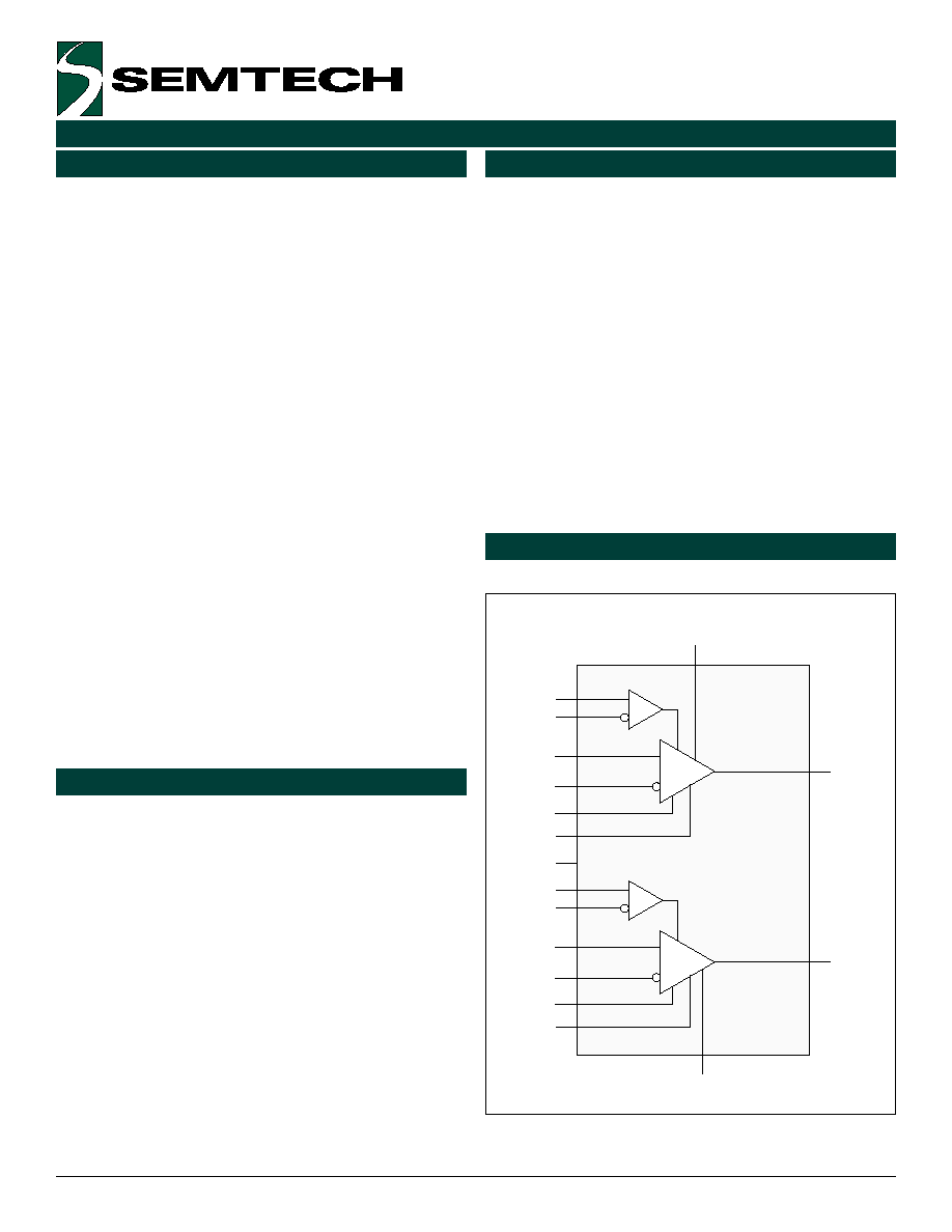
Functional Block Diagram
Applications
Revision 1 / March 31, 1998
The Edge692 is a dual pin electronics driver
manufactured in a high-performance, complementary
bipolar process. In Automatic Test Equipment (ATE)
applications, the Edge692 offers two pin drivers suitable
for drive-only channels in memory testers, as well as for
bidirectional channels in memory, VLSI, and mixed- signal
test systems.
The Edge692 is designed to produce excellent waveforms
(low overshoot), especially at low swings (<500 mV), and
have extremely low leakage currents in HiZ mode. In
addition, the Edge692 is pin and functionally compatible
with both the Edge693 and the Bt692.
Each driver is capable of forcing 9V signals over a 12V
range, in addition to going into a high impedance state.
The driver slew rate is adjustable between 2 V/ns and 1
V/ns.
Each driver is completely isolated from the other. There
are separate data, enable, slew rate adjust, high and
low levels, as well as power supply inputs for each driver.
Combining two independent drivers into a 28 pin PLCC
package offers a highly integrated solution where speed
and density are at a premium.
∑
2 V/ns Driver Slew Rates
∑
Adjustable Driver Slew Rates
∑
Three Statable
∑
Low HiZ Leakage
∑
Low Voltage Driver Swings
∑
Low Overshoot Waveforms
∑
12 V Output Range
∑
9 V Output Swings
∑
28-Pin PLCC with an Internal
Heat Spreader
∑
Edge693 Compatible
∑
Bt692 Compatible
EN
EN
SLEWADJA
SLEWADJB
DOUTA
DRIVER A
DRIVER B
DOUTB
DRVENA
DRVENA*
DHIA
DHIA*
DVHA
DVLA
DRVENB
DRVENB*
DHIB
DHIB*
DVHB
DVLB
BIAS
∑
Memory Test Equipment
∑
Instrumentation

2
2000 Semtech Corp.
www.semtech.com
EDGE HIGH-PERFORMANCE PRODUCTS
PIN Description
e
m
a
N
n
i
P
#
n
i
P
n
o
i
t
p
i
r
c
s
e
D
r
e
v
i
r
D
*
A
N
E
V
R
D
,
A
N
E
V
R
D
*
B
N
E
V
R
D
,
B
N
E
V
R
D
4
2
,
5
2
6
,
5
B
d
n
a
A
(
r
e
v
i
r
d
e
h
t
r
e
h
t
e
h
w
e
n
i
m
r
e
t
e
d
t
a
h
t
s
n
i
p
t
u
p
n
i
l
a
i
t
n
e
r
e
f
f
i
d
e
g
a
t
l
o
v
e
d
i
W
.
e
t
a
t
s
e
c
n
a
d
e
p
m
i
h
g
i
h
a
n
i
d
e
c
a
l
p
r
o
e
g
a
t
l
o
v
a
g
n
i
c
r
o
f
s
i
)
y
l
e
v
i
t
c
e
p
s
e
r
*
A
I
H
D
,
A
I
H
D
*
B
I
H
D
,
B
I
H
D
8
2
,
7
2
2
,
3
s
l
e
v
e
l
e
l
b
a
m
m
a
r
g
o
r
p
o
w
t
f
o
e
n
o
e
c
r
o
f
t
a
h
t
s
n
i
p
t
u
p
n
i
l
a
i
t
n
e
r
e
f
f
i
d
e
g
a
t
l
o
v
e
d
i
W
.
t
u
p
t
u
o
)
y
l
e
v
i
t
c
e
p
s
e
r
B
d
n
a
A
(
r
e
v
i
r
d
e
h
t
t
a
)
L
V
D
r
o
H
V
D
(
A
T
U
O
D
B
T
U
O
D
8
1
2
1
.
s
t
u
p
t
u
o
B
r
e
v
i
r
d
d
n
a
A
r
e
v
i
r
D
A
H
V
D
,
A
L
V
D
B
H
V
D
,
B
L
V
D
3
2
,
2
2
7
,
8
A
r
e
v
i
r
d
r
o
f
s
l
e
v
e
l
t
u
p
t
u
o
h
g
i
h
d
n
a
w
o
l
e
h
t
m
a
r
g
o
r
p
t
a
h
t
s
t
u
p
n
i
g
o
l
a
n
a
d
e
e
r
e
f
f
u
B
.
B
r
e
v
i
r
d
d
n
a
A
P
A
C
H
V
D
,
A
P
A
C
L
V
D
B
P
A
C
H
V
D
,
B
P
A
C
L
V
D
1
2
,
6
1
9
,
4
1
.
n
i
p
h
c
a
e
o
t
d
e
t
c
e
n
n
o
c
e
b
d
l
u
o
h
s
d
n
u
o
r
g
o
t
r
o
t
i
c
a
p
a
c
F
µ
1
0
.
0
.
s
n
i
p
g
o
l
a
n
A
A
J
D
A
W
E
L
S
B
J
D
A
W
E
L
S
0
2
0
1
d
n
a
A
r
e
v
i
r
d
f
o
s
e
t
a
r
w
e
l
s
l
l
a
f
d
n
a
e
s
i
r
e
h
t
t
s
u
j
d
a
t
a
h
t
s
t
u
p
n
i
t
n
e
r
r
u
c
g
o
l
a
n
A
.
B
r
e
v
i
r
d
S
A
I
B
1
r
o
f
l
e
v
e
l
s
a
i
b
l
a
n
r
e
t
n
i
e
h
t
s
t
e
s
e
d
o
n
s
i
h
t
o
t
n
i
t
n
e
r
r
u
c
e
v
i
t
i
s
o
p
A
.
t
u
p
n
i
g
o
l
a
n
A
.
B
r
e
v
i
r
d
d
n
a
A
r
e
v
i
r
d
r
e
w
o
P
B
E
E
V
,
A
E
E
V
3
1
,
7
1
.
B
r
e
v
i
r
d
d
n
a
A
r
e
v
i
r
d
r
o
f
y
l
p
p
u
s
r
e
w
o
p
e
v
i
t
a
g
e
N
B
C
C
V
,
A
C
C
V
1
1
,
9
1
.
B
r
e
v
i
r
d
d
n
a
A
r
e
v
i
r
d
r
o
f
y
l
p
p
u
s
r
e
w
o
p
e
v
i
t
i
s
o
P
B
D
N
G
,
A
D
N
G
4
,
6
2
.
B
r
e
v
i
r
d
d
n
a
A
r
e
v
i
r
d
r
o
f
d
n
u
o
r
g
e
c
i
v
e
D
s
n
i
P
t
s
e
T
E
D
O
I
D
L
A
M
R
E
H
T
5
1
.
e
r
u
t
a
r
e
p
m
e
t
n
o
i
t
c
n
u
j
e
i
d
e
h
t
k
c
a
r
t
o
t
d
e
s
u
t
u
p
t
u
o
r
o
t
i
n
o
m
l
a
m
r
e
h
T
3
2000 Semtech Corp.
www.semtech.com
EDGE HIGH-PERFORMANCE PRODUCTS
PIN Description (continued)
DOUTA
VEEA
DVLCAPA
THERMAL DIODE
DVLCAPB
VEEB
DOUTB
GNDA
DHIA
DHIA*
BIAS
DHIB*
DHIB
GNDB
DR
VENB
DR
VENB*
D
VHB
D
VLB
D
VHCAPB
SLEW
ADJB
VCCB
DR
VENA
DR
VENA*
D
VHA
D
VLA
D
VHCAP
A
SLEW
ADJ
A
VCCA
25
24
23
22
21
20
19
18
17
16
15
14
13
12
26
27
28
1
2
3
4
5
6
7
8
9
10
11
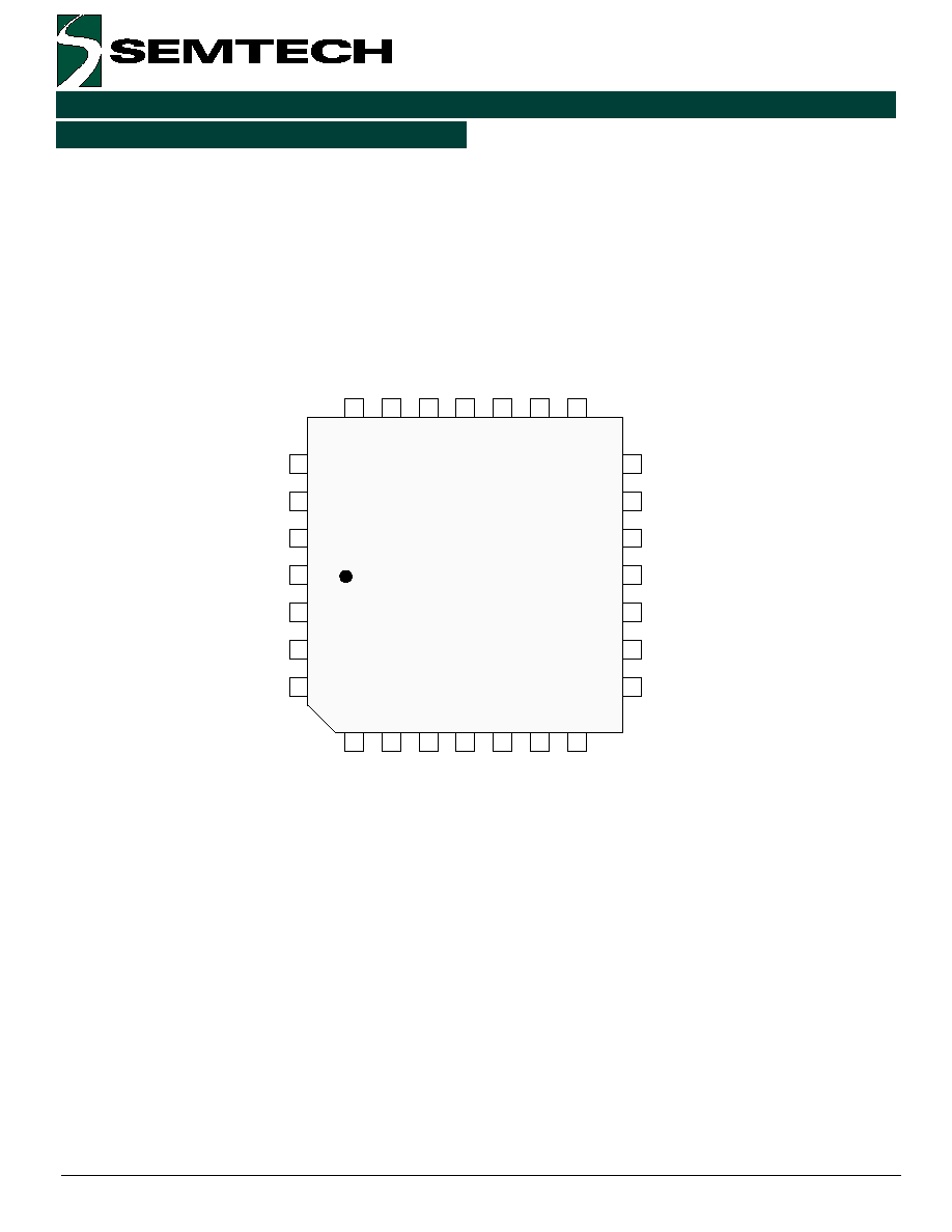
28-Pin PLCC
4
2000 Semtech Corp.
www.semtech.com
EDGE HIGH-PERFORMANCE PRODUCTS
Circuit Description
Introduction
The driver circuit will force the DOUT output to one of
three states:
1.
DVH (driver high voltage level)
2.
DVL (driver low voltage level)
3.
High Impedance (Hi Z).
Both driver digital control inputs (DHI/DHI*, DRVEN/
DRVEN*) are wide-voltage differential inputs capable of
receiving ECL, TTL, and CMOS signals. Single-ended
operation is achievable by generating the proper
threshold levels for the inverting inputs.
Drive Enable
The drive enable (DRVEN/DRVEN*) inputs control
whether the driver is forcing a voltage or is placed in a
high-impedance state. If DRVEN is more positive than
DRVEN*, the output will force either DVL or DVH,
depending on the driver data inputs. When DRVEN is
more negative than DRVEN*, the output is set to high-
impedance, independent of the driver data inputs.
Driver Data
The driver data inputs (DHI/DHI*) determine whether
the driver output is high or low. If DHI is more positive
than DHI*, the output will force DVH when the driver is
enabled. If DHI is more negative than DHI*, the output
will force DVL when the driver is enabled.
Table 1 summarizes the functionality of the driver enable
and driver data pins.
Table 1. DRVEN and DHI Pin Functionality
Driver Levels
DVH and DVL are high input impedance voltage controlled
inputs that establish the driver logical high and low levels
respectively.
DVLCAP / DVHCAP
These two analog nodes are brought out to better
stabilize the high and low driver levels. Much like placing
decoupling capacitors on the DVL and DVH input pins,
the DVLCAP and DVHCAP pins require a fixed .01
µ
F
chip capacitor (with good high frequency characteristics)
to ground. A tight layout with minimum etch is
recommended.
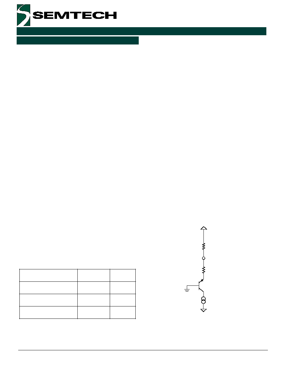
Driver Bias
The BIAS pin is an analog current input that establishes
a reference current for the driver and influences the
overall speed and power consumption of the chip. The
BIAS input current may be varied from 1.0 mA to 2.0
mA. Ideally, a current source would supply this current.
However, a resistor to a voltage source, typically VCC, is
acceptable.
The BIAS input structure is shown in Figure 1.
Figure 1. BIAS Input Structure
*
N
E
V
R
D
,
N
E
V
R
D
*
I
H
D
,
I
H
D
T
U
O
D
*
N
E
V
R
D
>
N
E
V
R
D
*
I
H
D
>
I
H
D
H
V
D
*
N
E
V
R
D
>
N
E
V
R
D
*
I
H
D
<
I
H
D
L
V
D
*
N
E
V
R
D
<
N
E
V
R
D
X
Z
i
H
50
REXT
BIAS
VCC
VEE
5
2000 Semtech Corp.
www.semtech.com
EDGE HIGH-PERFORMANCE PRODUCTS
Circuit Description (continued)
The desired value for the external resistor can be
determined from the relationship:
IBIAS = (VCC - .7) / (Rext + 50).
The actual IBIAS level is determined by selecting the
desired performance and power level. The charts listed
in the Application Information section enable the user
to quickly determine the appropriate bias level.
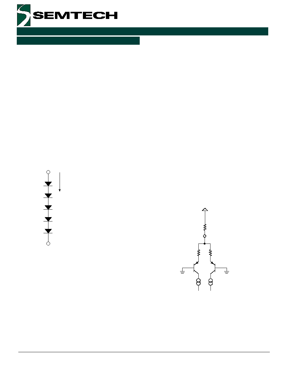
Thermal Monitor
The Edge692 includes an on-chip thermal monitor
accessible through the THERMAL DIODE pin. This node
connects to 5 diodes in series to VEE (see Figure 2) and
may be used to accurately measure the junction
temperature at any time.
Figure 2. Thermal Diode String
A bias current of 100
µ
A is injected into this node, and
the measured voltage corresponds to a specific junction
temperature with the following equation:
TJ(∞C) = {[(VTHERMAL DIODE ≠ VEE) / 5] ≠ .7} / (≠.00208).
Slew Rate Adjustment
The driver rising and falling slew rates are adjustable
from 2 V/ns to 1 V/ns. The actual slew rate realized is a
function of the chip bias and slew rate adjust input
currents.
The SLEWADJ input is determined by selecting the
desired performance and power level (after the BIAS
current is first chosen.) The charts listed in the
Application Information section enable the user to quickly
determine the appropriate SLEWADJ level.
SLEWADJ is a current controlled input that varies the
rising and falling edge slew rates. Ideally, a current DAC
would be used to establish this current. However, a
resistor to a positive voltage, typically VCC, is acceptable.
Figure 3 shows a simplified schematic of the SLEWADJ
input stage. Once a desired input current is selected,
the external resistor value is determined by the following
relationship:
(VCC - .7) / (Rext + 860) = Islewadj.
Figure 3. SLEWADJ input circuitry
Notice that the driver A slew rate and driver B slew rate
are independent. However, the rising and falling edge
slew rates on each driver track each other and are not
independent.
Bias Current
Temperature coefficient = ≠10 mV/
∞
C
Thermal Diode
VEE
1.72K
1.72K
REXT
SLEWADJ
VCC
Iradj
Ifadj
6
2000 Semtech Corp.
www.semtech.com
EDGE HIGH-PERFORMANCE PRODUCTS
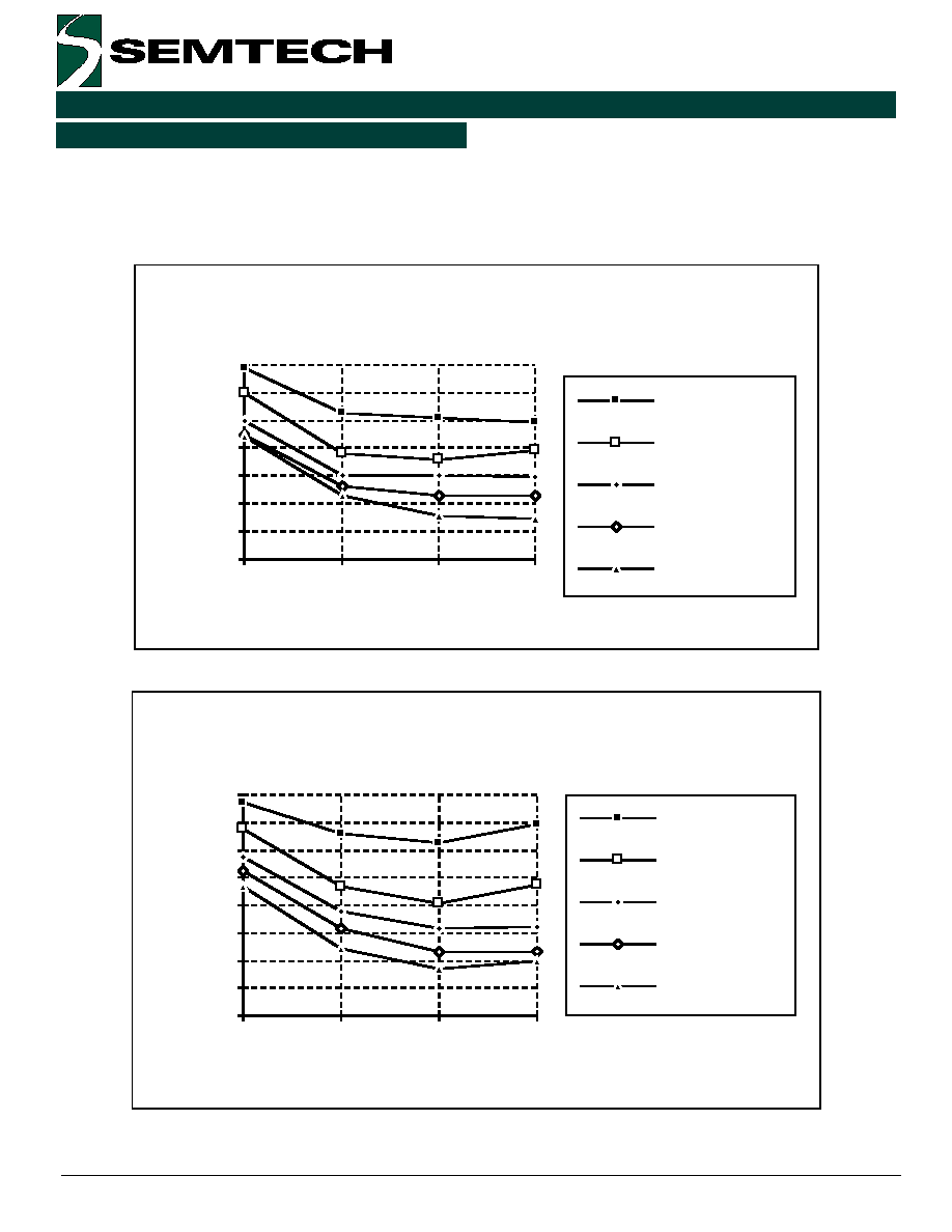
Application Information
Family of Curves for Rise and Fall Times for 800 mV Swings.
Rise Times for 800 mV Swings
Slewadj (mA)
Rise
Time
(ns)
0.4
0.45
0.5
0.55
0.6
0.65
0.7
0.75
1
1.4
1.8
2.2
Ibias = 1.0 mA
Ibias = 1.25 mA
Ibias = 1.5 mA
Ibias = 1.75 mA
Ibias = 2.0 mA
Fall Times for 800 mV Swings
Slewadj (mA)
Fall
Time
(ns)
0.45
0.5
0.55
0.6
0.65
0.7
0.75
0.8
0.85
1
1.4
1.8
2.2
Ibias = 1.0 mA
Ibias = 1.25 mA
Ibias = 1.5 mA
Ibias = 1.75 mA
Ibias = 2.0 mA
7
2000 Semtech Corp.
www.semtech.com
EDGE HIGH-PERFORMANCE PRODUCTS
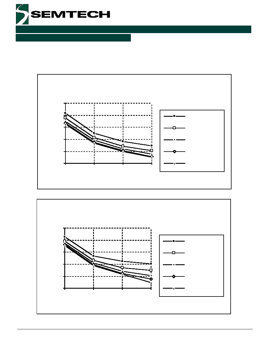
Application Information (continued)
Family of Curves for Rise and Fall Times for 3V Swings.
Rise Times for 3V Swings
Slewadj (mA)
Rise
Time
(ns)
1
1.5
2
2.5
3
3.5
1
1.4
1.8
2.2
Ibias = 1.0 mA
Ibias = 1.25 mA
Ibias = 1.5 mA
Ibias = 1.75 mA
Ibias = 2.0 mA
Fall Times for 3V Swings
Slewadj (mA)
Fall
Time
(ns)
1
1.5
2
2.5
3
3.5
1
1.4
1.8
2.2
Ibias = 1.0 mA
Ibias = 1.25 mA
Ibias = 1.5 mA
Ibias = 1.75 mA
Ibias = 2.0 mA

8
2000 Semtech Corp.
www.semtech.com
EDGE HIGH-PERFORMANCE PRODUCTS
Application Information (continued)
Family of Curves for Rise and Fall Times for 5V Swings.
Rise Times for 5V Swings
Slewadj (mA)
R
ise
Time
(ns)
2
2.5
3
3.5
4
4.5
5
5.5
1
1.4
1.8
2.2
Ibias = 1.0 mA
Ibias = 1.25
mA
Ibias = 1.5 mA
Ibias = 1.75
mA
Ibias = 2.0 mA
Fall Times for 5V Swings
Slewadj (mA)
Fall
Time
(ns)
2
2.5
3
3.5
4
4.5
5
5.5
1
1.4
1.8
2.2
Ibias = 1.0 mA
Ibias = 1.25 mA
Ibias = 1.5 mA
Ibias = 1.75 mA
Ibias = 2.0 mA
9
2000 Semtech Corp.
www.semtech.com
EDGE HIGH-PERFORMANCE PRODUCTS
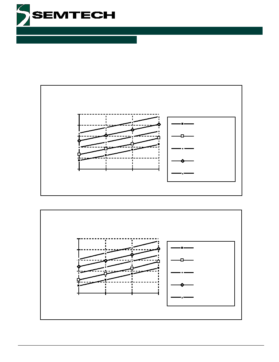
Application Information (continued)
Supply Current Family of Curves
Negative Supply Current
Slewadj (mA)
Iee
(mA)
60.00
80.00
100.00
120.00
140.00
160.00
1
1.4
1.8
2.2
Ibias = 1.0 mA
Ibias = 1.25 mA
Ibias = 1.5 mA
Ibias = 1.75 mA
Ibias = 2.0 mA
Positive Supply Current
Slewadj (mA)
Icc
(mA)
60.00
80.00
100.00
120.00
140.00
160.00
1
1.4
1.8
2.2
Ibias = 1.0 mA
Ibias = 1.25 mA
Ibias = 1.5 mA
Ibias = 1.75 mA
Ibias = 2.0 mA
10
2000 Semtech Corp.
www.semtech.com
EDGE HIGH-PERFORMANCE PRODUCTS
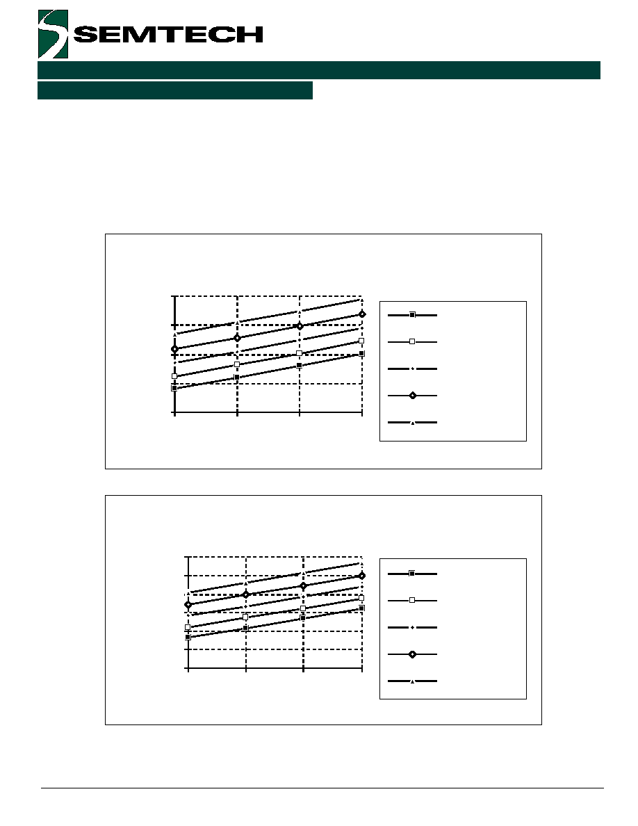
Application Information (continued)
Power Dissipation Family of Curves
Conditions:
VCC = +11.5V
VEE = ≠7.5V
Ta = 40∞C
JA = 26∞C
Quiescent Power Consumption
Slewadj (mA)
Pd
(Watts)
1.00
1.50
2.00
2.50
3.00
1
1.4
1.8
2.2
Ibias = 1.0 mA
Ibias = 1.25 mA
Ibias = 1.5 mA
Ibias = 1.75 mA
Ibias = 2.0 mA
Junction Temperature
Slewadj (mA)
T
j
(∞C)
60.00
70.00
80.00
90.00
100.00
110.00
120.00
1
1.4
1.8
2.2
Ibias = 1.0 mA
Ibias = 1.25 mA
Ibias = 1.5 mA
Ibias = 1.75 mA
Ibias = 2.0 mA

11
2000 Semtech Corp.
www.semtech.com
EDGE HIGH-PERFORMANCE PRODUCTS
Application Information (continued)
Thermal Information
r
e
t
e
m
a
r
a
P
l
o
b
m
y
S
n
i
M
p
y
T
x
a
M
s
t
i
n
U
e
c
n
a
t
s
i
s
e
R
l
a
m
r
e
h
T
e
s
a
C
o
t
n
o
i
t
c
n
u
J
C
J
3
1
o
W
/
C
r
i
A
o
t
n
o
i
t
c
n
u
J
r
i
A
l
l
i
t
S
M
P
F
L
0
5
M
P
F
L
0
0
4
A
J
A
J
A
J
9
4
6
3
6
2
o
W
/
C
o
W
/
C
o
W
/
C
12
2000 Semtech Corp.
www.semtech.com
EDGE HIGH-PERFORMANCE PRODUCTS
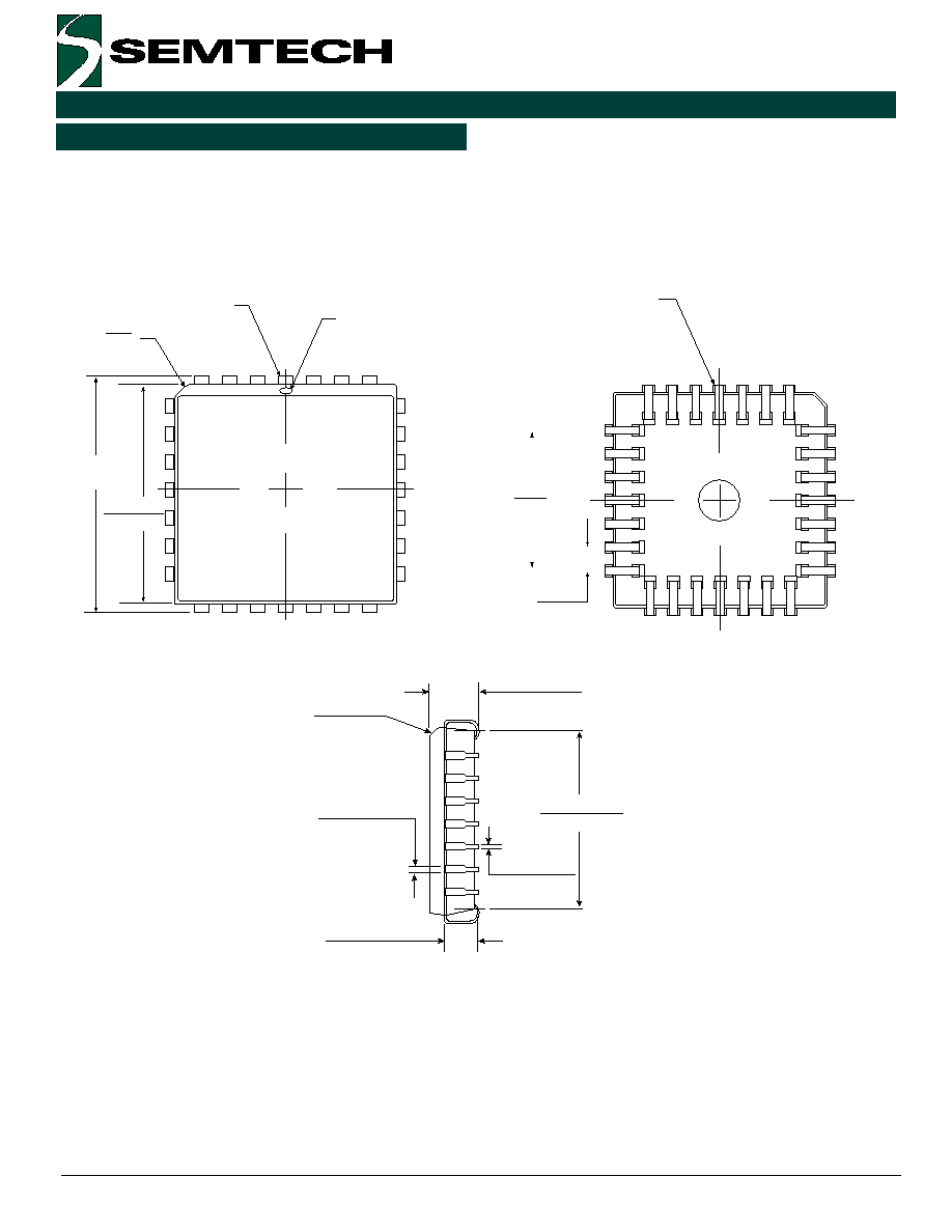
Package Information
PIN Descriptions
Pin #1
Pin #1 Ident
0.045 x 45
o
[1.143]
0.485 ≠ 0.495
[12.32 ≠ 12.57]
SQ
0.450 ≠ 0.456
[11.43 ≠ 11.58]
SQ
Pin #1
0.300 REF
[7.62]
0.050
[1.27]
TYP
0.026 ≠ 0.032
[0.661 ≠ 0.812]
0.026 ≠ 0.032
[0.661 ≠ 0.812]
0.090 ≠ 0.120
[2.29 ≠ 3.04]
0.390 ≠ 0430
[9.91 ≠ 10.92]
0.165 ≠ 0.180
[4.19 ≠ 4.57]
.045 x 45
o
[1.14]
28 Pin PLCC Package
JA = 75 to 80∞C / W
Notes: (unless otherwise specified)
1.
Dimensions are in inches [millimeters].
2.
Tolerances are: .XXX
±
0.005 [0.127].
3.
PLCC packages are intended for surface mounting on solder lands on 0.050 [1.27] centers.

13
2000 Semtech Corp.
www.semtech.com
EDGE HIGH-PERFORMANCE PRODUCTS
Recommended Operating Conditions
Absolute Maximum Ratings
r
e
t
e
m
a
r
a
P
l
o
b
m
y
S
n
i
M
p
y
T
x
a
M
s
t
i
n
U
y
l
p
p
u
S
r
e
w
o
P
e
v
i
t
i
s
o
P
C
C
V
5
.
8
5
.
1
1
5
.
3
1
V
y
l
p
p
u
S
r
e
w
o
P
e
v
i
t
a
g
e
N
E
E
V
5
.
8
-
5
.
7
-
2
.
4
-
V
y
l
p
p
u
S
g
o
l
a
n
A
l
a
t
o
T
E
E
V
-
C
C
V
7
.
2
1
0
.
9
1
V
s
t
u
p
n
I
g
o
l
a
n
A
l
e
v
e
L
h
g
i
H
r
e
v
i
r
D
l
e
v
e
L
w
o
L
r
e
v
i
r
D
s
a
i
B
r
e
v
i
r
D
t
s
u
j
d
A
e
t
a
R
w
e
l
S
A
r
e
v
i
r
D
t
s
u
j
d
A
e
t
a
R
w
e
l
S
B
r
e
v
i
r
D
H
V
D
L
V
D
S
A
I
B
A
J
D
A
W
E
L
S
B
J
D
A
W
E
L
S
5
.
3
+
E
E
V
9
.
2
+
E
E
V
0
.
1
0
.
1
0
.
1
5
.
1
5
7
.
1
5
7
.
1
9
.
2
-
C
C
V
5
.
3
-
C
C
V
0
.
2
2
.
2
2
.
2
V
V
A
m
A
m
A
m
e
r
u
t
a
r
e
p
m
e
T
g
n
i
t
a
r
e
p
O
t
n
e
i
b
m
A
A
T
5
2
+
0
7
+
o
C
e
r
u
t
a
r
e
p
m
e
T
n
o
i
t
c
n
u
J
J
T
5
2
+
5
2
1
+
o
C
r
e
t
e
m
a
r
a
P
l
o
b
m
y
S
n
i
M
p
y
T
x
a
M
s
t
i
n
U
)
D
N
G
o
t
e
v
i
t
a
l
e
R
(
C
C
V
C
C
V
0
0
.
4
1
+
V
D
N
G
o
t
e
v
i
t
a
l
e
R
(
E
E
V
E
E
V
0
.
0
1
-
0
V
y
l
p
p
u
S
r
e
w
o
P
l
a
t
o
T
E
E
V
-
C
C
V
0
.
0
2
+
V
s
e
g
a
t
l
o
V
t
u
p
n
I
l
a
t
i
g
i
D
*
N
E
V
R
D
,
N
E
V
R
D
*
I
H
D
,
I
H
D
E
E
V
0
.
6
+
V
s
e
g
a
t
l
o
V
t
u
p
n
I
l
a
i
t
n
e
r
e
f
f
i
D
*
N
E
V
R
D
-
N
E
V
R
D
*
I
H
D
-
I
H
D
0
.
5
-
0
.
5
+
V
s
e
g
a
t
l
o
V
g
o
l
a
n
A
H
V
D
,
L
V
D
,
T
U
O
D
E
E
V
C
C
V
V
s
t
n
e
r
r
u
C
t
u
p
n
I
g
o
l
a
n
A
s
a
i
B
r
e
v
i
r
D
t
s
u
j
d
A
e
t
a
R
w
e
l
S
S
A
I
B
A
J
D
A
W
E
L
S
B
J
D
A
W
E
L
S
0
0
0
6
.
2
8
.
2
8
.
2
A
m
A
m
A
m
e
r
u
t
a
r
e
p
m
e
T
g
n
i
t
a
r
e
p
O
t
n
e
i
b
m
A
A
T
5
5
-
5
2
1
+
o
C
e
r
u
t
a
r
e
p
m
e
T
e
g
a
r
o
t
S
S
T
5
6
-
0
5
1
+
o
C
e
r
u
t
a
r
e
p
m
e
T
n
o
i
t
c
n
u
J
J
T
0
5
1
+
o
C
e
r
u
t
a
r
e
p
m
e
T
g
n
i
r
e
d
l
o
S
)
n
i
p
m
o
r
f
"
4
/
1
,
s
d
n
o
c
e
s
5
(
L
O
S
T
0
6
2
o
C
Thermal equilibrium is established by applying power for at least 2 minutes while maintaining a transverse
air flow of 400 linear feet per minute over the device mounted either in the test socket or on the printed
circuit board. Thermal resistance measurements are taken with device soldered to PCB.

14
2000 Semtech Corp.
www.semtech.com
EDGE HIGH-PERFORMANCE PRODUCTS
DC Characteristics
r
e
t
e
m
a
r
a
P
l
o
b
m
y
S
n
i
M
p
y
T
x
a
M
s
t
i
n
U
t
i
u
c
r
i
C
r
e
v
i
r
D
t
n
e
r
r
u
C
t
u
p
n
I
g
o
l
a
n
A
L
V
D
,
H
V
D
t
u
p
n
I
s
a
i
B
N
I
I
S
A
I
B
0
0
2
-
0
.
1
5
.
1
0
0
2
+
0
.
2
A
µ
A
m
s
t
u
p
n
I
t
n
e
m
t
s
u
j
d
A
e
g
n
a
R
t
n
e
r
r
u
C
J
D
A
W
E
L
S
0
.
1
5
7
.
1
2
.
2
A
m
t
i
u
c
r
i
C
r
e
v
i
r
D
e
g
n
a
R
e
g
a
t
l
o
V
t
u
p
t
u
O
g
n
i
w
S
e
g
a
t
l
o
V
t
u
p
t
u
O
:
t
n
e
r
r
u
C
t
u
p
t
u
O
c
i
t
a
t
S
x
a
M
V
2
-
>
T
U
O
D
V
2
-
<
T
U
O
D
t
n
e
r
r
u
C
t
u
p
t
u
O
c
i
m
a
n
y
D
x
a
M
)
1
e
t
o
N
(
t
n
e
r
r
u
C
e
g
a
k
a
e
L
T
U
O
D
T
U
O
D
V
g
n
i
w
s
V
T
U
O
D
I
T
U
O
D
I
K
A
E
L
I
5
.
3
+
E
E
V
0
5
3
-
0
2
-
0
0
1
-
1
-
5
2
0
.
<
5
.
3
-
C
C
V
0
.
9
5
3
+
0
2
+
0
0
1
+
1
V
V
A
m
A
m
A
m
A
µ
y
c
a
r
u
c
c
A
C
D
h
g
i
H
r
e
v
i
r
D
)
2
e
t
o
N
(
t
e
s
f
f
O
)
3
e
t
o
N
(
n
i
a
G
)
4
e
t
o
N
(
y
t
i
r
a
e
n
i
L
T
U
O
D
-
H
V
D
/
H
V
D
T
U
O
D
T
U
O
D
-
L
V
D
0
5
1
-
5
9
.
0
2
-
9
9
.
0
1
<
0
5
3
0
.
1
0
2
V
m
V
/
V
V
m
w
o
L
r
e
v
i
r
D
)
2
e
t
o
N
(
t
e
s
f
f
O
)
3
e
t
o
N
(
n
i
a
G
)
4
e
t
o
N
(
y
t
i
r
a
e
n
i
L
T
U
O
D
-
H
V
D
/
H
V
D
T
U
O
D
T
U
O
D
-
L
V
D
0
5
1
-
5
9
.
0
2
-
9
9
.
0
1
<
0
5
3
0
.
1
0
2
V
m
V
/
V
V
m
e
r
u
t
a
r
e
p
m
e
T
e
g
a
t
l
o
V
t
e
s
f
f
O
t
n
e
i
c
i
f
f
e
o
C
C
T
T
U
O
D
1
±
/
V
m
o
C
e
c
n
a
d
e
p
m
I
t
u
p
t
u
O
r
e
v
i
r
D
T
U
O
Z
0
.
1
0
.
3
5
.
4
R
R
S
P
r
e
v
i
r
D
R
R
S
P
0
3
B
d
s
t
u
p
n
I
l
a
t
i
g
i
D
*
I
H
D
,
I
H
D
,
*
N
E
V
R
D
,
N
E
V
R
D
t
n
e
r
r
u
C
t
u
p
n
I
e
g
n
a
R
e
g
a
t
l
o
V
t
u
p
n
I
g
n
i
w
S
t
u
p
n
I
l
a
i
t
n
e
r
e
f
f
i
D
N
I
I
G
N
R
V
F
F
I
D
V
0
0
9
-
0
.
2
-
5
2
.
0
0
0
9
+
5
.
5
+
0
.
4
+
A
µ
V
V
t
n
e
r
r
u
C
y
l
p
p
u
S
r
e
w
o
P
y
l
p
p
u
S
e
v
i
t
i
s
o
P
y
l
p
p
u
S
e
v
i
t
a
g
e
N
C
C
I
E
E
I
0
5
1
-
0
2
1
0
2
1
0
5
1
A
m
A
m
Note 1:
Device output leakage is specified with DOUT over the entire output voltage range.
Note 2:
The offset voltage is defined as the difference between the measured driver output at DOUT under no
load conditions versus the programmed voltage (DVH or DVL) when forced to ≠1.0 V.
Note 3:
The driver gain is defined as the change in driver output voltage (DOUT) divided by the change in
programmed input voltage (DVH or DVL). Measurements are taken at ≠1.0 V and +4.0 V programmed
inputs with the output under no-load conditions.
Note 4:
Linearity error is defined as the maximum deviation between the theoretical driver output voltage
(predicted by the straight line determined by the offset and gain) and the actual measured output
voltage under no load conditions.

15
2000 Semtech Corp.
www.semtech.com
EDGE HIGH-PERFORMANCE PRODUCTS
AC Characteristics
r
e
t
e
m
a
r
a
P
l
o
b
m
y
S
n
i
M
p
y
T
x
a
M
s
t
i
n
U
t
i
u
c
r
i
C
r
e
v
i
r
D
)
1
e
t
o
N
(
T
U
O
D
o
t
I
H
D
m
o
r
f
d
p
T
d
p
T
7
.
1
s
n
)
2
e
t
o
N
(
Z
i
H
T
U
O
D
o
t
N
E
V
R
D
m
o
r
f
d
p
T
7
.
1
s
n
)
2
e
t
o
N
(
e
v
i
t
c
A
T
U
O
D
o
t
N
E
V
R
D
m
o
r
f
d
p
T
7
.
1
s
n
)
3
e
t
o
N
(
s
e
m
i
T
l
l
a
F
/
e
s
i
R
T
U
O
D
%
0
8
-
%
0
2
,
V
m
0
0
8
%
0
9
-
%
0
1
,
V
3
%
0
9
-
%
0
1
,
V
5
f
T
/
r
T
f
T
/
r
T
f
T
/
r
T
5
.
5
2
.
1
5
2
.
2
6
.
0
6
.
1
5
7
.
2
5
7
.
0
.
3
0
.
5
s
n
s
n
s
n
e
t
a
R
e
l
g
g
o
T
V
m
0
0
8
V
3
V
5
x
a
m
F
0
0
2
0
5
1
0
0
1
z
H
M
z
H
M
z
H
M
Z
i
H
n
i
e
c
n
a
t
i
c
a
p
a
C
t
u
p
t
u
O
t
u
o
C
0
.
2
F
p
)
4
e
t
o
N
(
h
t
d
i
W
e
s
l
u
P
m
u
m
i
n
i
M
V
m
0
0
8
V
3
V
5
5
.
2
0
.
3
0
.
5
s
n
s
n
s
n
The specified limits shown can be met only after thermal equilibrium has been established. Thermal
equilibrium is established by applying power for at least two minutes while maintaining the normal operating
environment.
Note 1:
Tpd is measured from crossover point of DHI and DHI* to the 50% point in the output. DVL
equals 0 V and DVH equals +3 V.
Note 2:
Specification condition: DVL equals -1 V and DVH equals +1 V. Output is terminated to GND by
100
.
Tpd is measured from the crossover point of DRVEN and DRVEN* to the point where a
10-percent change in output voltage occurs.
Note 3:
The driver load is an 18" 50
.
transmission line terminated with 1K
.
in parallel with 2 pF.
Note 4:
The output pulse width is measured at the 50-percent points. Output reaches 100% of programmed
value.

16
2000 Semtech Corp.
www.semtech.com
EDGE HIGH-PERFORMANCE PRODUCTS
Ordering Information
Contact Information
Semtech Corporation
Edge High-Performance Division
10021 Willow Creek Rd., San Diego, CA 92131
Phone: (858)695-1808 FAX (858)695-2633
r
e
b
m
u
N
l
e
d
o
M
e
g
a
k
c
a
P
e
r
u
t
a
r
e
p
m
e
T
t
n
e
i
b
m
A
e
g
n
a
R
J
H
A
2
9
6
E
C
C
L
P
n
i
P
-
8
2
)
r
e
d
a
e
r
p
S
t
a
e
H
l
a
n
r
e
t
n
I
h
t
i
w
(
5
2
+
o
0
7
+
o
t
C
o
C
J
H
A
2
9
6
M
V
E
e
l
u
d
o
M
n
o
i
t
a
u
l
a
v
E
2
9
6
e
g
d
E