
PROTECTION PRODUCTS
1
www.semtech.com
PROTECTION PRODUCTS
LC03-3.3
Low Capacitance 3.3 Volt TVS
for High Speed Interfaces
1800 watts peak pulse power (t
p
= 8/20µs)
Transient protection for high-speed data lines to
Bellcore 1089 (Intra-Building) 100A (2/10µs)
ITU K.20 I
PP
=40A (5/310µs)
IEC 61000-4-2 (ESD) ±15kV (air), ±8kV (contact)
IEC 61000-4-4 (EFT) 40A (5/50ns)
IEC 61000-4-5 (Lightning) 100A (8/20µs)
Protects two lines in common and differential mode
Low capacitance for high-speed interfaces
Low operating voltage (3.3V)
Low clamping voltage
Integrated structure saves board space and
increases reliability
Solid-state EPD technology
Description
Features
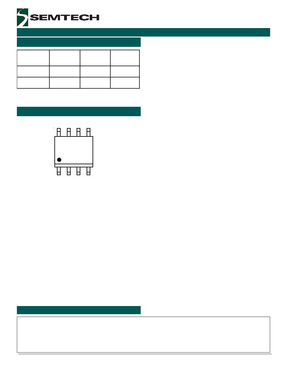
Circuit Diagram
Schematic & PIN Configuration
Revision 10/14/04
Applications
Mechanical Characteristics
SO-8 (Top View)
The LC03-3.3 transient voltage suppressor is designed
to protect components which are connected to high
speed data and telecommunication lines from voltage
surges caused by lightning, electrostatic discharge
(ESD), and electrical fast transients (EFT).
TVS diodes are ideal for use as board level protection
of sensitive semiconductor components. The LC03-
3.3 combines a TVS diode with a rectifier bridge to
provide transient protection in both common and
differential mode with a single device. The LC03-3.3
utilizes Semtech's EPD technology for superior electri-
cal characteristics at 3.3 volts. The capacitance of the
device is minimized to ensure correct signal transmis-
sion on high speed lines.
The LC03-3.3 meets the short-haul (intra-building)
transient immunity requirements of Bellcore 1089 for
telecommunications applications.
JEDEC SO-8 package
Molding compound flammability rating: UL 94V-0
Marking : Part number, date code
Packaging : Tube or Tape and Reel per EIA 481
Low Voltage Interfaces
T3/E3
10/100/1000 Ethernet
Set-Top Box
ISDN Interfaces
1
2
3
4
5
6
7
8
Pin 1 and 8
Pin 4 and 5
Pin 2, 3,
6, and 7
Ground
2
2004 Semtech Corp.
www.semtech.com
PRELIMINARY
PROTECTION PRODUCTS
LC03-3.3
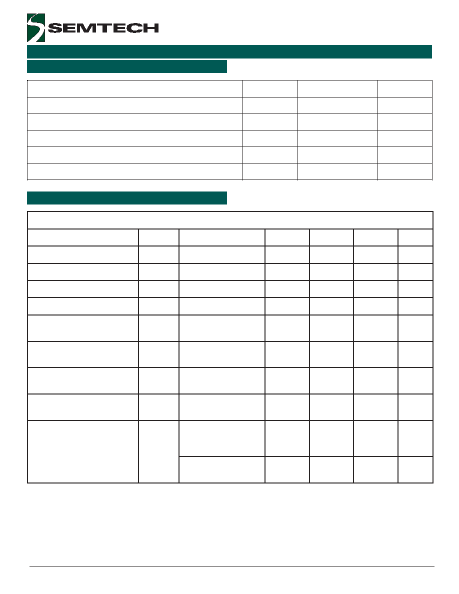
Absolute Maximum Rating
Electrical Characteristics
g
n
i
t
a
R
l
o
b
m
y
S
e
u
l
a
V
s
t
i
n
U
t
(
r
e
w
o
P
e
s
l
u
P
k
a
e
P
p
)
s
µ
0
2
/
8
=
P
k
p
0
0
8
1
s
t
t
a
W
t
(
t
n
e
r
r
u
C
e
s
l
u
P
k
a
e
P
p
)
s
µ
0
2
/
8
=
I
P
P
0
0
1
A
e
r
u
t
a
r
e
p
m
e
T
g
n
ir
e
d
l
o
S
d
a
e
L
T
L
).
c
e
s
0
1
(
0
6
2
C
∞
e
r
u
t
a
r
e
p
m
e
T
g
n
it
a
r
e
p
O
T
J
5
2
1
+
o
t
5
5
-
C
∞
e
r
u
t
a
r
e
p
m
e
T
e
g
a
r
o
t
S
T
G
T
S
0
5
1
+
o
t
5
5
-
C
∞
3
.
3
-
3
0
C
L
r
e
t
e
m
a
r
a
P
l
o
b
m
y
S
s
n
o
i
t
i
d
n
o
C
m
u
m
i
n
i
M
l
a
c
i
p
y
T
m
u
m
i
x
a
M
s
t
i
n
U
e
g
a
tl
o
V
f
f
O
-
d
n
a
t
S
e
s
r
e
v
e
R
V
M
W
R
3
.
3
V
e
g
a
tl
o
V
h
g
u
o
r
h
T
-
h
c
n
u
P
V
T
P
I
T
P
A
µ
2
=
5
.
3
V
e
g
a
tl
o
V
k
c
a
B
-
p
a
n
S
V
B
S
I
B
S
A
m
0
5
=
8
.
2
V
t
n
e
r
r
u
C
e
g
a
k
a
e
L
e
s
r
e
v
e
R
I
R
V
M
W
R
C
∞
5
2
=
T
,
V
3
.
3
=
1
A
µ
e
g
a
tl
o
V
g
n
i
p
m
a
l
C
V
C
I
P
P
t
,
A
0
5
=
p
s
µ
0
2
/
8
=
d
n
u
o
r
G
-
o
t-
e
n
i
L
5
.
1
1
V
e
g
a
tl
o
V
g
n
i
p
m
a
l
C
V
C
I
P
P
t
,
A
0
5
=
p
s
µ
0
2
/
8
=
e
n
i
L
-
o
t-
e
n
i
L
5
.
3
1
V
e
g
a
tl
o
V
g
n
i
p
m
a
l
C
V
C
I
P
P
t
,
A
0
0
1
=
p
s
µ
0
2
/
8
=
d
n
u
o
r
G
-
o
t-
e
n
i
L
5
1
V
e
g
a
tl
o
V
g
n
i
p
m
a
l
C
V
C
I
P
P
t
,
A
0
0
1
=
p
s
µ
0
2
/
8
=
e
n
i
L
-
o
t-
e
n
i
L
8
1
V
e
c
n
a
ti
c
a
p
a
C
n
o
it
c
n
u
J
C
j
d
n
a
s
n
i
p
O
/
I
n
e
e
w
t
e
B
d
n
u
o
r
G
V
R
z
H
M
1
=
f
,
V
0
=
6
1
5
2
F
p
s
n
i
p
O
/
I
n
e
e
w
t
e
B
V
R
z
H
M
1
=
f
,
V
0
=
8
2
1
F
p
3
2004 Semtech Corp.
www.semtech.com
PROTECTION PRODUCTS
PROTECTION PRODUCTS
LC03-3.3
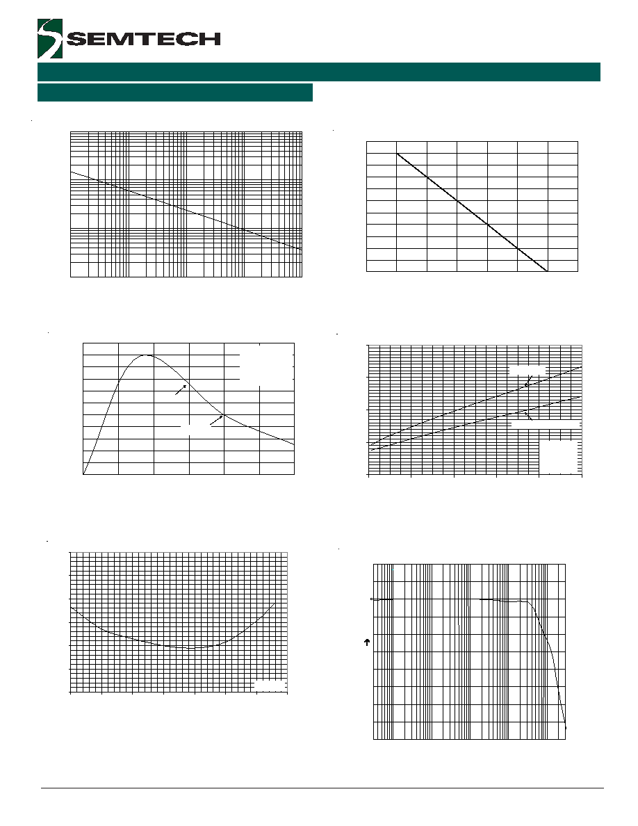
Typical Characteristics
Non-Repetitive Peak Pulse Power vs. Pulse Time
Power Derating Curve
Clamping Voltage vs. Peak Pulse Current
0
10
20
30
40
50
60
70
80
90
100
110
0
5
10
15
20
25
30
Time (µs)
Pe
r
cen
t o
f
I
PP
e
-t
td = I
PP
/2
Waveform
Parameters:
tr = 8µs
td = 20µs
Pulse Waveform
Capacitance vs. Reverse Voltage
0
10
20
30
40
50
60
70
80
90
100
110
0
25
50
75
100
125
150
175
Ambient Temperature - T
A
(
o
C)
%
of
Ra
t
e
d P
o
w
e
r or I
PP
0
5
10
15
20
0
20
40
60
80
100
Peak Pulse Current - I
PP
(A)
C
l
a
m
ping
V
o
lt
a
g
e
-
V
C
(V)
Waveform
Parameters:
tr = 8µs
td = 20µs
Line-To-Ground
Line-To-Line
7
7.5
8
8.5
9
9.5
10
0
0.5
1
1.5
2
2.5
3
3.5
Reverse Voltage - V
R
(V)
C
a
p
aci
t
a
n
c
e -
C
j
(
pF)
f = 1MHz
0.1
1
10
100
0.1
1
10
100
1000
Pulse Duration - t
p
(µs)
Pe
a
k
Pu
l
s
e
Po
w
e
r
- P
pk
(k
W
)
Insertion Loss S21
(Line to Ground)
CH1 S21 LOG
3 dB/ REF 0 dB
START . 030 MHz
3
STOP 000 . 000 000 MHz
4
2004 Semtech Corp.
www.semtech.com
PRELIMINARY
PROTECTION PRODUCTS
LC03-3.3
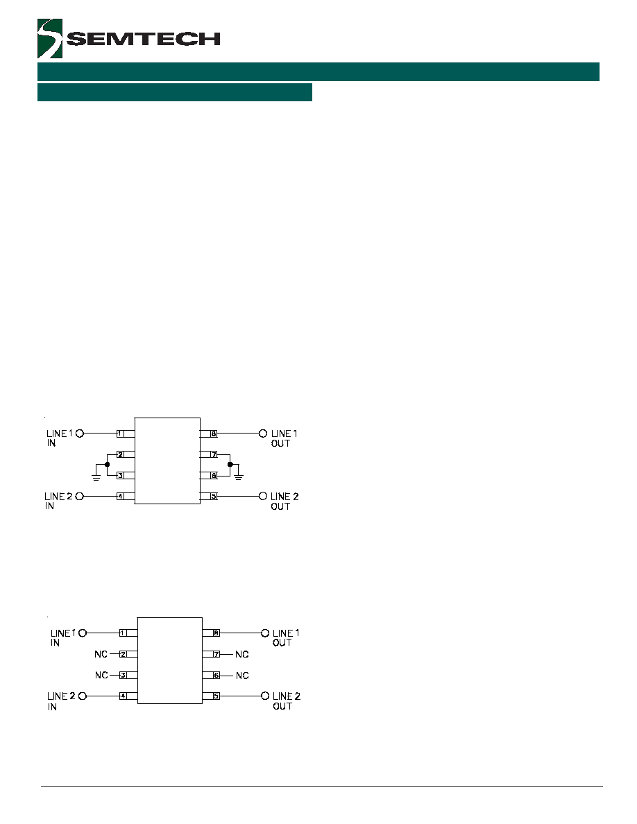
Connection for Differential (Line-to-Line) and Com-
mon Mode Protection (Line-to-Ground)
Device Connection Options for Protection of Two
High-Speed Data Lines
The LC03-3.3 is designed to protect two high-speed
data lines (one differential pair) from transient over-
voltages which result from lightning and ESD. The
device can be configured to protect in differential (Line-
to-Line) and common (Line-to-Ground) mode. Data line
inputs/outputs are connected at pins 1 to 8, and 4 to
5 as shown. Pins 2, 3, 6, and 7 are connected to
ground. These pins should be connected directly to a
ground plane on the board for best results. The path
length is kept as short as possible to minimize parasitic
inductance. In applications where high common mode
voltages are present, differential protection is achieved
by leaving pins 2, 3, 6, and 7 not connected.
Connection for Differential Protection
(Line-to-Line)
Applications Information
Matte Tin Lead Finish
Matte tin has become the industry standard lead-free
replacement for SnPb lead finishes. A matte tin finish
is composed of 100% tin solder with large grains.
Since the solder volume on the leads is small com-
pared to the solder paste volume that is placed on the
land pattern of the PCB, the reflow profile will be
determined by the requirements of the solder paste.
Therefore, these devices are compatible with both
lead-free and SnPb assembly techniques. In addition,
unlike other lead-free compositions, matte tin does not
have any added alloys that can cause degradation of
the solder joint.

5
2004 Semtech Corp.
www.semtech.com
PROTECTION PRODUCTS
PROTECTION PRODUCTS
LC03-3.3
Bellcore 1089 Intra-Building Protection Gigabit Ethernet
Typical Applications
6
2004 Semtech Corp.
www.semtech.com
PRELIMINARY
PROTECTION PRODUCTS
LC03-3.3
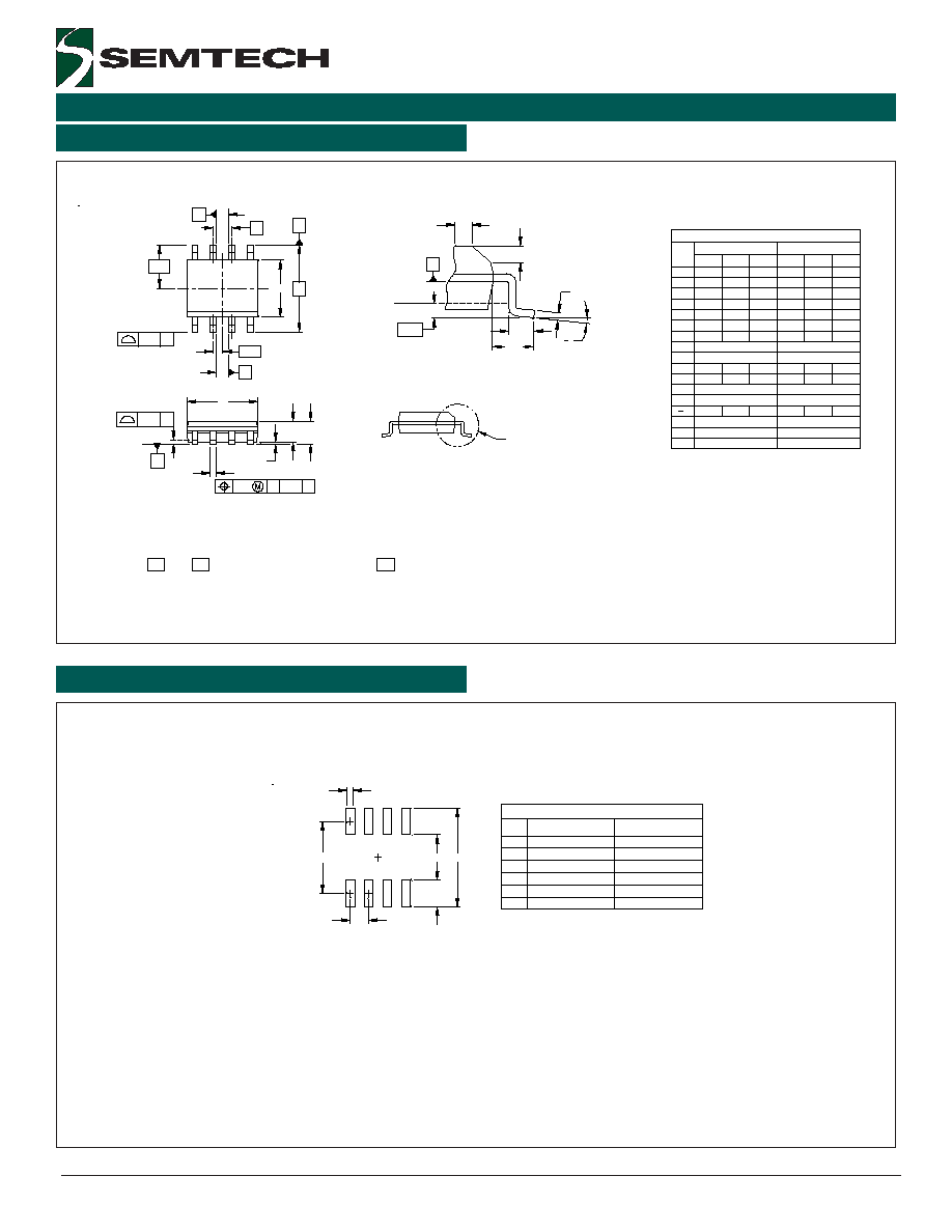
Land Pattern -SO-8
Outline Drawing - SO-8
bxN
2X N/2 TIPS
SEATING
aaa C
E/2
2X
1
2
N
A
D
A1
E1
bbb
C A-B D
ccc C
e/2
A2
SEE DETAIL
A
SIDE VIEW
A
B
C
D
e
DETAIL
A
c
L
(L1)
01
0.25
GAGE
PLANE
h
h
H
PLANE
3. DIMENSIONS "E1" AND "D" DO NOT INCLUDE MOLD FLASH, PROTRUSIONS
OR GATE BURRS.
-B-
CONTROLLING DIMENSIONS ARE IN MILLIMETERS (ANGLES IN DEGREES).
DATUMS AND TO BE DETERMINED AT DATUM PLANE
NOTES:
1.
2.
-A-
-H-
REFERENCE JEDEC STD MS-012, VARIATION AA.
4.
.050 BSC
.236 BSC
8
.010
.150
.189
.154
.193
.012
-
8
0.25
1.27 BSC
6.00 BSC
3.90
4.90
-
.157
.197
3.80
4.80
.020 0.31
4.00
5.00
0.51
(.041)
.004
.008
-
.028
-
-
-
-
0∞
.016
.007
.049
.004
.053
8∞
0∞
0.20
0.10
-
8∞
0.40
0.17
1.25
0.10
.041
.010
.069
.065
.010
1.35
(1.04)
0.72
-
1.04
0.25
-
-
-
1.75
1.65
0.25
0.25
-
.010
.020
0.50
-
L1
N
01
bbb
aaa
ccc
A
b
A2
A1
D
E
E1
L
h
e
c
DIM
MIN
MILLIMETERS
NOM
DIMENSIONS
INCHES
MIN
MAX
MAX
NOM
E
(.205)
(5.20)
Z
G
Y
P
(C)
3.00
.118
1.27
.050
0.60
.024
2.20
.087
7.40
.291
X
INCHES
DIMENSIONS
Z
P
Y
X
DIM
C
G
MILLIMETERS
THIS LAND PATTERN IS FOR REFERENCE PURPOSES ONLY.
CONSULT YOUR MANUFACTURING GROUP TO ENSURE YOUR
COMPANY'S MANUFACTURING GUIDELINES ARE MET.
NOTES:
1.
REFERENCE IPC-SM-782A, RLP NO. 300A.
2.
7
2004 Semtech Corp.
www.semtech.com
PROTECTION PRODUCTS
PROTECTION PRODUCTS
LC03-3.3
Contact Information
Semtech Corporation
Protection Products Division
200 Flynn Road, Camarillo, CA 93012
Phone: (805)498-2111 FAX (805)498-3804
r
e
b
m
u
N
t
r
a
P
h
s
i
n
i
F
d
a
e
L
r
e
p
y
t
Q
l
e
e
R
e
z
i
S
l
e
e
R
B
T
.
3
.
3
-
3
0
C
L
b
P
n
S
0
0
5
h
c
n
I
7
T
B
T
.
3
.
3
-
3
0
C
L
e
e
r
F
b
P
0
0
5
h
c
n
I
7
Ordering Information
SC YYWW
LC03-3.3
Marking Diagram
Note:
YYWW = Date Code