 | –≠–ª–µ–∫—Ç—Ä–æ–Ω–Ω—ã–π –∫–æ–º–ø–æ–Ω–µ–Ω—Ç: LCDA15-1 | –°–∫–∞—á–∞—Ç—å:  PDF PDF  ZIP ZIP |
PROTECTION PRODUCTS
PRELIMINARY
1
www.semtech.com
PROTECTION PRODUCTS
LCDA15-1
Low Capacitance TVS Diode Array
Description
Features
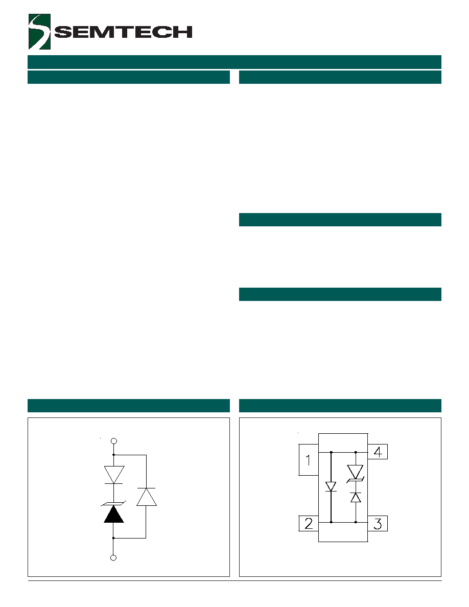
Circuit Diagram
Schematic & PIN Configuration
Revision 01/15/03
The LCDA15-1 is a low capacitance transient voltage
suppressor (TVS) diode array. It is designed to protect
sensitive CMOS ICs from the damaging effects of ESD
and lightning. Each device will protect one line in
common (line-to-ground) mode. They are low capaci-
tance (< 15pF) making them suitable for use on high-
speed telecom and datacom interfaces without signal
degradation.
The configuration of the LCDA15-1 has been optimized
for easy layout on high density boards. The small SOT-
143 package minimizes required board space. These
devices will handle up to 15 Amps for an 8/20µs
lightning impulse. The low inductance construction
minimizes voltage overshoot during high current
surges.
The LCDA15-1 may be used to protect ADSL inter-
faces, portable electronics, and wireless systems.
Applications
Mechanical Characteristics
ADSL Interfaces
Serial/Parallel Interfaces
High-Speed Data Lines
Portable Electronics
WAN/LAN Equipment
Wireless Systems
Transient protection for high-speed data lines to
IEC 61000-4-2 (ESD) ±15kV (air), ±8kV (contact)
IEC 61000-4-4 (EFT) 40A (5/50ns)
IEC 61000-4-5 (lightning) 15A (8/20µs)
Configuration optimized for easy board layout
Protects one line
Low capacitance (<15pF) for high-speed interfaces
Low clamping voltage
Low leakage current
Operating voltage: 15V
Solid-state silicon-avalanche technology
JEDEC SOT-143 package
Molding compound flammability rating: UL 94V-0
Marking : Marking code
Packaging : Tape and Reel per EIA 481
SOT-143 (Top View)
2
2003 Semtech Corp.
www.semtech.com
PROTECTION PRODUCTS
PROTECTION PRODUCTS
LCDA15-1
Absolute Maximum Rating
Electrical Characteristics
g
n
i
t
a
R
l
o
b
m
y
S
e
u
l
a
V
s
t
i
n
U
t
(
r
e
w
o
P
e
s
l
u
P
k
a
e
P
p
)
s
µ
0
2
/
8
=
P
k
p
0
0
5
s
t
t
a
W
t
(
t
n
e
r
r
u
C
e
s
l
u
P
k
a
e
P
p
)
s
µ
0
2
/
8
=
I
P
P
5
1
A
e
r
u
t
a
r
e
p
m
e
T
g
n
ir
e
d
l
o
S
d
a
e
L
T
L
).
c
e
s
0
1
(
0
6
2
C
∞
e
r
u
t
a
r
e
p
m
e
T
g
n
it
a
r
e
p
O
T
J
5
2
1
+
o
t
5
5
-
C
∞
e
r
u
t
a
r
e
p
m
e
T
e
g
a
r
o
t
S
T
G
T
S
0
5
1
+
o
t
5
5
-
C
∞
1
-
5
1
A
D
C
L
r
e
t
e
m
a
r
a
P
l
o
b
m
y
S
s
n
o
i
t
i
d
n
o
C
m
u
m
i
n
i
M
l
a
c
i
p
y
T
m
u
m
i
x
a
M
s
t
i
n
U
e
g
a
tl
o
V
f
f
O
-
d
n
a
t
S
e
s
r
e
v
e
R
V
M
W
R
5
1
V
e
g
a
tl
o
V
n
w
o
d
k
a
e
r
B
e
s
r
e
v
e
R
V
R
B
I
t
A
m
1
=
7
.
6
1
V
t
n
e
r
r
u
C
e
g
a
k
a
e
L
e
s
r
e
v
e
R
I
R
V
M
W
R
C
∞
5
2
=
T
,
V
5
1
=
5
A
µ
e
g
a
tl
o
V
d
r
a
w
r
o
F
e
d
o
i
D
g
n
ir
e
e
t
S
V
F
I
F
A
1
=
5
.
1
V
e
g
a
tl
o
V
g
n
i
p
m
a
l
C
V
C
I
P
P
t
,
A
1
=
p
s
µ
0
2
/
8
=
4
2
V
e
g
a
tl
o
V
g
n
i
p
m
a
l
C
V
C
I
P
P
t
,
A
5
1
=
p
s
µ
0
2
/
8
=
3
3
V
e
c
n
a
ti
c
a
p
a
C
n
o
it
c
n
u
J
C
j
d
n
a
s
n
i
p
O
/
I
n
e
e
w
t
e
B
d
n
u
o
r
G
V
R
z
H
M
1
=
f
,
V
0
=
8
5
1
F
p
3
2003 Semtech Corp.
www.semtech.com
PROTECTION PRODUCTS
PRELIMINARY
PROTECTION PRODUCTS
LCDA15-1
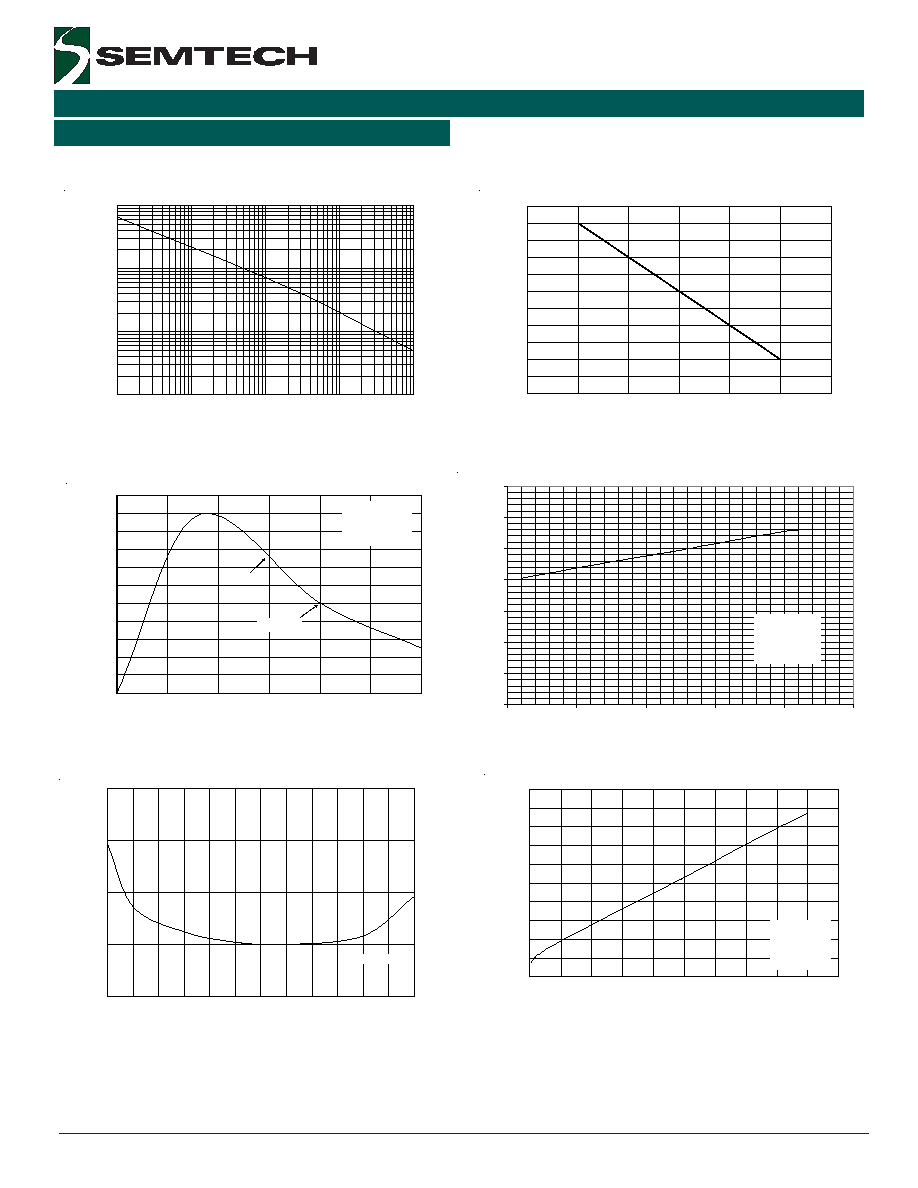
Typical Characteristics
Non-Repetitive Peak Pulse Power vs. Pulse Time
Power Derating Curve
0
10
20
30
40
50
60
70
80
90
100
110
0
25
50
75
100
125
150
Ambient Temperature - T
A
(
o
C)
% of Rated Power or I
PP
Clamping Voltage vs. Peak Pulse Current
0
10
20
30
40
50
60
70
80
90
100
110
0
5
10
15
20
25
30
T im e (µs)
P
e
r
cen
t o
f
I
PP
e
-
t
td = I
PP
/2
W aveform
Parameters:
tr = 8µ s
td = 20µ s
Pulse Waveform
Capacitance vs. Reverse Voltage
0.01
0.1
1
10
0.1
1
10
100
1000
Pulse Duration - t
p
(µs)
P
eak
P
u
l
s
e
P
o
w
e
r
-
P
pk
(kW)
Forward Voltage vs. Forward Current
0
5
10
15
20
25
30
35
0
5
10
15
20
25
Peak P ulse C u rren t - I
PP
(A)
C
l
a
m
ping
V
o
lt
a
g
e
-
V
C
(V)
W aveform
Parameters:
tr = 8µ s
td = 20µ s
7
7 . 5
8
8 . 5
9
0
1
2
3
4
5
6
7
8
9
1 0
1 1
1 2
R e v e r s e V o lt a g e - V
R
( V )
Ca
p
a
c
i
ta
n
c
e
-
C
j
(p
F
)
f= 1 M H z
0
1
2
3
4
5
6
7
8
9
10
0
5
10
15
20
25
30
35
40
45
50
Forward Current - I
F
(A)
F
o
r
w
ar
d
V
o
l
t
ag
e -
V
F
(V)
Waveform
Parameters:
tr = 8µs
td = 20µs

4
2003 Semtech Corp.
www.semtech.com
PROTECTION PRODUCTS
PROTECTION PRODUCTS
LCDA15-1
Applications Information
Device Connection for Protection of High-Speed Data
Lines
The LCDA15-1 is designed to protect high-speed data
lines from transient over-voltages which result from
lightning and ESD. The device is designed to protect
one unidirectional line in common mode (Line-to-
Ground). For common mode protection, The signal is
input at pins 2 and 3. Pins 1 and 4 are connected to
ground. The ground connection should be made
directly to the ground plane for best results.
ADSL Protection
Figure 2 shows a typical ADSL schematic diagram with
the LCDA15-1 configured to provide lightning and ESD
protection for the sensitive ADSL line driver. The
LCDA15-1 is connected from each line to ground on
the IC side of the line. The LCDA15-1 should to be
grounded to the system ground to provide a proper
reference.
1
2
3
4
Line
In
Line
Out
Figure 1 - Connection for Common Mode
Protection (Line-to-Ground)
Figure 2 - ADSL Protection Circuit
LCDA15-1
+15
+15
LCDA15-1

5
2003 Semtech Corp.
www.semtech.com
PROTECTION PRODUCTS
PRELIMINARY
PROTECTION PRODUCTS
LCDA15-1
Land Pattern - SOT-143
Outline Drawing - SOT-143
Notes:
(1) Controlling dimension: Inch (unless otherwise specified).
(2) Dimension A and B do not include mold protrusions. Mold protrusions are .006" max.