RClamp0504N.pmd
1
www.semtech.com
PROTECTION PRODUCTS - RailClamp
RClamp0504N
RailClamp
Low Capacitance TVS Diode Array
Description
Features
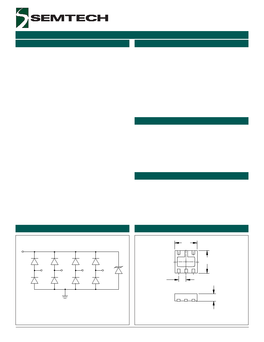
Circuit Diagram
Package Dimensions
Revision 01/20/2005
RailClamps are surge rated diode arrays designed to
protect high speed data interfaces. The RClamp series
has been specifically designed to protect sensitive
components which are connected to data and trans-
mission lines from overvoltage caused by electrostatic
discharge (ESD), electrical fast transients (EFT), and
lightning.
The unique design of the RClamp series devices
incorporates eight surge rated, low capacitance steer-
ing diodes and a TVS in a single package. During
transient conditions, the steering diodes direct the
transient to either the positive side of the power supply
line or to ground. The internal TVS diode prevents
over-voltage on the power line, protecting any down-
stream components.
The RClamp
TM
0504N has a low typical capacitance of
3pF and operates with virtually no insertion loss to
1GHz. This makes the device ideal for protection of
high-speed data lines such as USB 2.0, Firewire, DVI,
and gigabit Ethernet interfaces.
The RClamp0504N is in a 6-pin, RoHs compliant,
SLP2020P6 package. It measures 2.0 x 2.0 x
0.60mm. The leads are spaced at a pitch of 0.5mm
and are finished with lead-free NiPd. Each device may
be used to protect four high-speed data or transmis-
sion lines. They may be used to meet the ESD immu-
nity requirements of IEC 61000-4-2, Level 4 (±15kV
air, ±8kV contact discharge).
Applications
Mechanical Characteristics
USB 2.0 Power and Data Line Protection
Video Graphics Cards
Monitors and Flat Panel Displays
Digital Video Interface (DVI)
10/100/1000 Ethernet
Notebook Computers
ESD protection for high-speed data lines to
IEC 61000-4-2 (ESD) ±15kV (air), ±8kV (contact)
IEC 61000-4-4 (EFT) 40A (5/50ns)
IEC 61000-4-5 (Lightning) 12A (8/20µs)
Array of surge rated diodes with internal TVS Diode
Small package saves board space
Protects four I/O lines
Low capacitance: 3pF typical
Low clamping voltage
Low operating voltage: 5.0V
Solid-state silicon-avalanche technology
SLP2020P6 Package
RoHs Compliant
Nominal Dimensions: 2.0 x 2.0 x 0.60 mm
Lead Pitch: 0.65mm
Lead Finish: NiPd
Marking : Marking Code and Date Code
Packaging : Tape and Reel per EIA 481
2.00
1
0.65 BSC
0.60
2.00
6 Pin SLP package (Bottom Side View)
Nominal Dimensions in mm
Device Schematic
Pin 5
Pin 1
Pin 3
Pin 4
Pin 6
Pin 2

2
2005 Semtech Corp.
www.semtech.com
PROTECTION PRODUCTS
RClamp0504N
Absolute Maximum Rating
N
4
0
5
0
p
m
a
l
C
R
r
e
t
e
m
a
r
a
P
l
o
b
m
y
S
s
n
o
i
t
i
d
n
o
C
m
u
m
i
n
i
M
l
a
c
i
p
y
T
m
u
m
i
x
a
M
s
t
i
n
U
e
g
a
tl
o
V
f
f
O
-
d
n
a
t
S
e
s
r
e
v
e
R
V
M
W
R
2
o
t
5
n
i
P
5
V
e
g
a
tl
o
V
n
w
o
d
k
a
e
r
B
e
s
r
e
v
e
R
V
R
B
I
t
A
m
1
=
2
o
t
5
n
i
P
6
V
t
n
e
r
r
u
C
e
g
a
k
a
e
L
e
s
r
e
v
e
R
I
R
V
M
W
R
C
°
5
2
=
T
,
V
5
=
2
o
t
5
n
i
P
5
A
µ
e
g
a
tl
o
V
d
r
a
w
r
o
F
V
F
I
f
A
m
5
1
=
2
.
1
V
e
g
a
tl
o
V
g
n
i
p
m
a
l
C
V
C
I
P
P
s
µ
0
2
/
8
=
p
t
,
A
1
=
d
n
u
o
r
G
o
t
n
i
p
O
/
I
y
n
A
5
.
2
1
V
e
g
a
tl
o
V
g
n
i
p
m
a
l
C
V
C
I
P
P
s
µ
0
2
/
8
=
p
t
,
A
5
=
d
n
u
o
r
G
o
t
n
i
p
O
/
I
y
n
A
5
.
7
1
V
e
c
n
a
ti
c
a
p
a
C
n
o
it
c
n
u
J
C
j
V
R
z
H
M
1
=
f
,
V
0
=
d
n
u
o
r
G
o
t
n
i
p
O
/
I
y
n
A
3
5
F
p
V
R
z
H
M
1
=
f
,
V
0
=
s
n
i
p
O
/
I
n
e
e
w
t
e
B
5
.
1
F
p
g
n
i
t
a
R
l
o
b
m
y
S
e
u
l
a
V
s
t
i
n
U
)
s
µ
0
2
/
8
=
p
t
(
r
e
w
o
P
e
s
l
u
P
k
a
e
P
P
k
p
0
0
3
s
t
t
a
W
)
s
µ
0
2
/
8
=
p
t
(
t
n
e
r
r
u
C
e
s
l
u
P
k
a
e
P
I
P
P
2
1
A
)
r
i
A
(
2
-
4
-
0
0
0
1
6
C
E
I
r
e
p
D
S
E
)
t
c
a
t
n
o
C
(
2
-
4
-
0
0
0
1
6
C
E
I
r
e
p
D
S
E
V
D
S
E
5
1
8
V
k
e
r
u
t
a
r
e
p
m
e
T
g
n
it
a
r
e
p
O
T
J
5
2
1
+
o
t
5
5
-
C
°
e
r
u
t
a
r
e
p
m
e
T
e
g
a
r
o
t
S
T
G
T
S
0
5
1
+
o
t
5
5
-
C
°
Electrical Characteristics (T = 25
o
C)
3
2005 Semtech Corp.
www.semtech.com
PROTECTION PRODUCTS
RClamp0504N
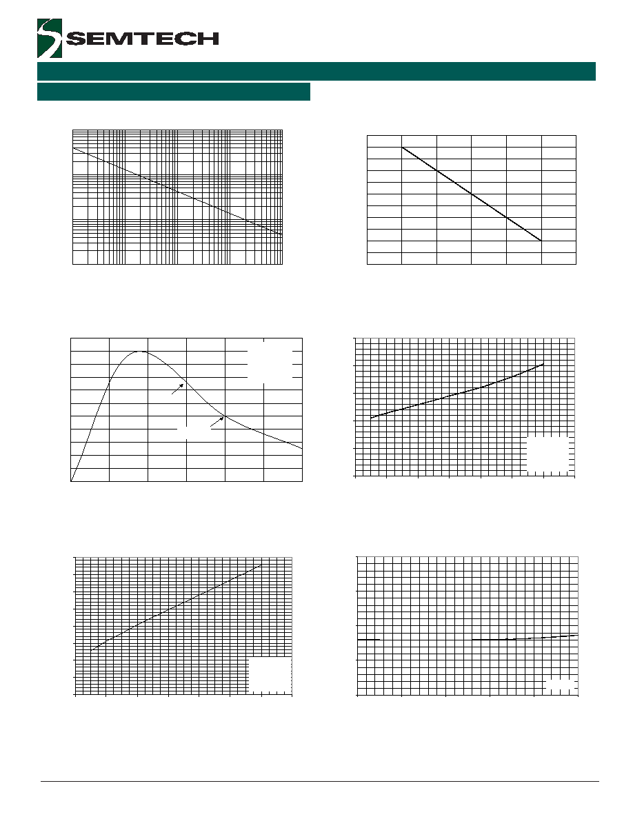
Typical Characteristics
Non-Repetitive Peak Pulse Power vs. Pulse Time
Power Derating Curve
0
10
20
30
40
50
60
70
80
90
100
110
0
25
50
75
100
125
150
Ambient Temperature - T
A
(
o
C)
%
of
Ra
t
e
d P
o
w
e
r or I
PP
Clamping Voltage vs. Peak Pulse Current
Pulse Waveform
Forward Voltage vs. Forward Current
Capacitance vs. Reverse Voltage
0.01
0.1
1
10
0.1
1
10
100
1000
Pulse Duration - tp (µs)
Peak
Pu
l
se Po
w
e
r
-
P
Pk
(k
W
)
0
10
20
30
40
50
60
70
80
90
100
110
0
5
10
15
20
25
30
Time (µs)
Per
c
en
t
of
I
PP
e
-t
td = I
PP
/2
Waveform
Parameters:
tr = 8µs
td = 20µs
0
5
10
15
20
25
0
2
4
6
8
10
12
14
Peak Pulse Current - I
PP
(A)
Cl
amp
i
n
g
V
o
l
t
ag
e -
V
C
(V)
Waveform
Parameters:
tr = 8µs
td = 20µs
0
0.5
1
1.5
2
2.5
3
3.5
4
0
2
4
6
8
10
12
14
Forward Current - I
F
(A)
Fo
r
w
a
r
d
V
o
lt
a
g
e
-
V
F
(V)
Waveform
Parameters:
tr = 8µs
td = 20µs
3
3.5
4
4.5
5
0
1
2
3
4
5
Reverse Voltage - V
R
(V)
C
a
p
aci
t
a
n
ce -
Cj
(
p
F
)
f = 1MHz
4
2005 Semtech Corp.
www.semtech.com
PROTECTION PRODUCTS
RClamp0504N
Device Connection Options for Protection of Four
High-Speed Data Lines
This device is designed to protect four data lines from
transient over-voltages by clamping them to a fixed
reference. When the voltage on the protected line
exceeds the reference voltage (plus diode V
F
) the
steering diodes are forward biased, conducting the
transient current away from the sensitive circuitry.
Data lines are connected at pins 1, 3, 4 and 6. The
negative reference is connected at pin 2. This pin
should be connected directly to a ground plane on the
board for best results. The path length is kept as short
as possible to minimize parasitic inductance.
The positive reference is connected at pin 5. The
options for connecting the positive reference are as
follows:
1. To protect data lines and the power line, connect
pin 5 directly to the positive supply rail (V
CC
). In this
configuration the data lines are referenced to the
supply voltage. The internal TVS diode prevents
over-voltage on the supply rail.
2. In applications where the supply rail does not exit
the system, the internal TVS may be used as the
reference. In this case, pin 5 is not connected.
The steering diodes will begin to conduct when the
voltage on the protected line exceeds the working
voltage of the TVS (plus one diode drop).3.
Applications Information
Vcc
In 1
In 2
In 3
In 4
1
NC
In 1
In 2
In 3
In 4
1
ESD Protection With RailClamps
RailClamps are optimized for ESD protection using the
rail-to-rail topology. Along with good board layout,
these devices virtually eliminate the disadvantages of
using discrete components to implement this topology.
Consider the situation shown in Figure 1 where dis-
crete diodes or diode arrays are configured for rail-to-
rail protection on a high speed line. During positive
duration ESD events, the top diode will be forward
biased when the voltage on the protected line exceeds
the reference voltage plus the V
F
drop of the diode.
For negative events, the bottom diode will be biased
when the voltage exceeds the V
F
of the diode. At first
approximation, the clamping voltage due to the charac-
teristics of the protection diodes is given by:
V
C
= V
CC
+ V
F
(for positive duration pulses)
V
C
= -V
F
(for negative duration pulses)
However, for fast rise time transient events, the
effects of parasitic inductance must also be consid-
ered as shown in Figure 2. Therefore, the actual
clamping voltage seen by the protected circuit will be:
V
C
= V
CC
+ V
F
+ L
P
di
ESD
/dt (for positive duration pulses)
V
C
= -V
F
- L
G
di
ESD
/dt
(for negative duration pulses)
ESD current reaches a peak amplitude of 30A in 1ns
for a level 4 ESD contact discharge per IEC 61000-4-2.
Figure 1 - "Rail-
Figure 1 - "Rail-
Figure 1 - "Rail-
Figure 1 - "Rail-
Figure 1 - "Rail-TTTTTo-Rail" Pr
o-Rail" Pr
o-Rail" Pr
o-Rail" Pr
o-Rail" Proooootttttection T
ection T
ection T
ection T
ection Topology
opology
opology
opology
opology
(First Approximation)
(First Approximation)
(First Approximation)
(First Approximation)
(First Approximation)
5
2005 Semtech Corp.
www.semtech.com
PROTECTION PRODUCTS
RClamp0504N
PIN Descriptions
Therefore, the voltage overshoot due to 1nH of series
inductance is:
V = L
P
di
ESD
/dt = 1X10
-9
(30 / 1X10
-9
) = 30V
Example:
Consider a V
CC
= 5V, a typical V
F
of 30V (at 30A) for the
steering diode and a series trace inductance of 10nH.
The clamping voltage seen by the protected IC for a
positive 8kV (30A) ESD pulse will be:
V
C
= 5V + 30V + (10nH X 30V/nH) = 335V
This does not take into account that the ESD current is
directed into the supply rail, potentially damaging any
components that are attached to that rail. Also note
that it is not uncommon for the V
F
of discrete diodes to
exceed the damage threshold of the protected IC. This
is due to the relatively small junction area of typical
discrete components. It is also possible that the
power dissipation capability of the discrete diode will
be exceeded, thus destroying the device.
The RailClamp is designed to overcome the inherent
disadvantages of using discrete signal diodes for ESD
suppression. The RailClamp's integrated TVS diode
helps to mitigate the effects of parasitic inductance in
the power supply connection. During an ESD event,
the current will be directed through the integrated TVS
diode to ground. The maximum voltage seen by the
protected IC due to this path will be the clamping
voltage of the device.
Applications Information (continued)
Figure 2 - The Effects of Parasitic Inductance
Figure 2 - The Effects of Parasitic Inductance
Figure 2 - The Effects of Parasitic Inductance
Figure 2 - The Effects of Parasitic Inductance
Figure 2 - The Effects of Parasitic Inductance
When Using Discrete Components to Implement
When Using Discrete Components to Implement
When Using Discrete Components to Implement
When Using Discrete Components to Implement
When Using Discrete Components to Implement
Rail-
Rail-
Rail-
Rail-
Rail-TTTTTo-Rail Pr
o-Rail Pr
o-Rail Pr
o-Rail Pr
o-Rail Proooootttttection
ection
ection
ection
ection
Figure 3 - Rail-
Figure 3 - Rail-
Figure 3 - Rail-
Figure 3 - Rail-
Figure 3 - Rail-TTTTTo-Rail Pr
o-Rail Pr
o-Rail Pr
o-Rail Pr
o-Rail Proooootttttection Using
ection Using
ection Using
ection Using
ection Using
RailClam
RailClam
RailClam
RailClam
RailClamp T
p T
p T
p T
p T VVVVVS Arra
S Arra
S Arra
S Arra
S Arrays
ys
ys
ys
ys
ETHERNET PROTECTION
Ethernet ICs are vulnerable to damage from electro-
static discharge (ESD), lightning, and cable discharge
events (CDE). The internal protection in the PHY chip,
if any, often is not enough due to the high energy of
these disturbances. The fatal discharge can occur
differentially across the transmit or receive line pair or
between any line and ground (common mode).
Common mode and differential mode protection
against ESD and CDE discharges can be achieved by
connecting the RClamp0504N on the PHY side of the
Ethernet circuit as shown in Figure 4. Pins 1, 3, 4, and
6 are connected to the transmit and receive line pairs.
Since there is no Vcc connection at the connector, pin
5 of the RClamp0504N should not be connected. Pin
2 is connected to ground. This connection should be
made directly to the ground plane. All path lengths
should be kept as short as possible to minimize para-
sitic inductance. This configuration can be used to
meet the ESD immunity requirements of IEC 61000-4-
2, cable discharge events, and tertiary lightning (up to
12A 8/20
µ
s). For enhanced lightning immunity to the
requirements of Telcordia GR-1089, a LC03-3.3 is
added across each line pair on the connector side of
the circuit (Figure 5). The LC03-3.3 provides differen-
tial lightning protection while the common mode
isolation of the transformer is relied upon for common
mode protection.