 | ÐлекÑÑоннÑй компоненÑ: SC1116 | СкаÑаÑÑ:  PDF PDF  ZIP ZIP |
SC1116 data sheet
POWER MANAGEMENT
1
www.semtech.com
SC1116
Linear FET Controller
For DDR Supplies
Features
Revision: October 22, 2003
Description
The SC1116 is a low cost controller for low power
linear DDR power supplies.
The SC1116 comes in a space saving SOT-23 6 pin
package.
The SC1116 provides a dual gate drive for the top se-
rial and bottom parallel MOSFETs with internal shoot
through protection.
The wide range of input voltages (3V to 15V) allows the
chip to work in many various applications.
The variable output voltage is programmable from the
outside with an input divider or an external reference.
DDR supplies
SCSI
Line termination
Source / Sink LDOs
User can select FETs to optimize system current
rating/dropout/cost
-40°C to +85°C
External compensation capable for low ESR loads
Minimum external components
0.6 mA Quiescent current
Guaranteed no shoot through
SOT-23 6L small package
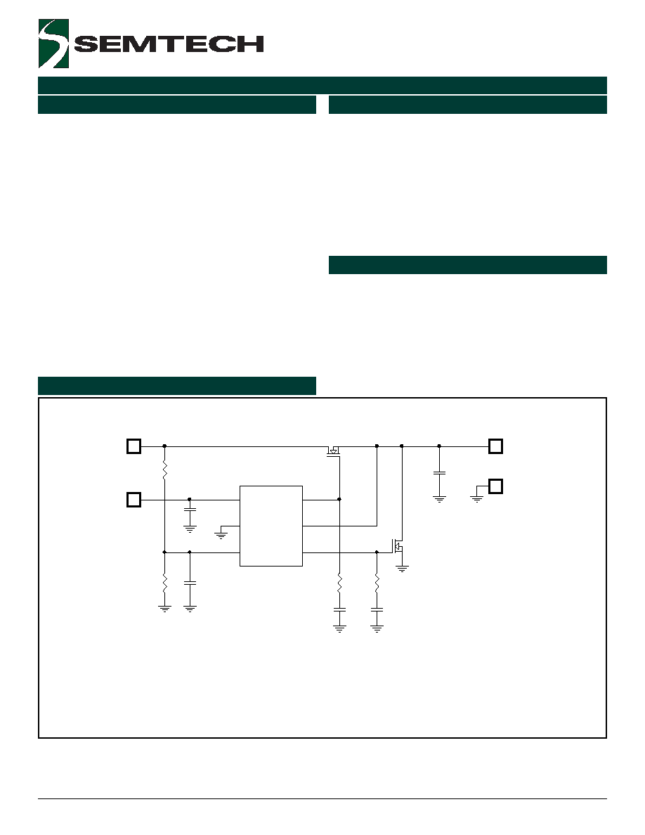
Typical Application Circuit
Applications
Notes:
(1) Values used for optional compensation are 1K and 4.7nF typical.
(2) When using 3V as Vcc, use of low threshold FETs is a must.
REF
3
DRVL
4
VCC
1
FB
5
GND
2
DRVH
6
U 1
SC1116
0 .1uF
0 .1uF
typ
4 .7nF
typ
4 .7nF
typ
4 7uF
R1
1k 0.5%
R2
1k 0.5%
typ
1k
typ
1k
Q1
MOS FET N
Q2
MOS FET N
VDDQ=2.5Vtyp
Vcc=3 to 15V
VTT=1.25Vtyp
GND
2
2003 Semtech Corp.
www.semtech.com
POWER MANAGEMENT
SC1116
Electricial Characteristics
r
e
t
e
m
a
r
a
P
s
n
o
i
t
i
d
n
o
C
t
s
e
T
n
i
M
p
y
T
x
a
M
s
t
i
n
U
e
g
a
tl
o
V
y
l
p
p
u
S
3
5
1
V
n
o
it
a
l
u
g
e
R
d
a
o
L
)
1
(
A
2
+
0
:
L
I
A
2
-
0
:
L
I
1
-
1
+
%
t
n
e
r
r
u
C
y
b
d
n
a
t
S
/t
n
e
r
r
u
C
t
n
e
c
s
e
i
u
Q
V
C
C
A
0
=
d
a
o
l
o
n
,
V
5
1
=
0
0
6
0
0
8
A
µ
e
v
i
r
D
e
t
a
G
w
o
L
t
u
p
t
u
O
I
K
N
I
S
A
m
5
.
2
=
5
1
.
0
5
2
.
0
V
h
g
i
H
t
u
p
t
u
O
I
E
C
R
U
O
S
A
m
5
.
2
=
5
2
.
0
-
c
c
V
5
1
.
0
-
c
c
V
V
r
e
t
e
m
a
r
a
P
l
o
b
m
y
S
m
u
m
i
x
a
M
s
t
i
n
U
e
g
a
tl
o
V
y
l
p
p
u
S
t
u
p
n
I
V
C
C
5
.
6
1
+
o
t
3
.
0
-
V
e
g
n
a
R
e
r
u
t
a
r
e
p
m
e
T
t
n
e
i
b
m
A
g
n
it
a
r
e
p
O
T
A
5
8
+
o
t
0
4
-
C
°
e
g
n
a
R
e
r
u
t
a
r
e
p
m
e
T
n
o
it
c
n
u
J
g
n
it
a
r
e
p
O
T
J
5
2
1
+
o
t
0
4
-
C
°
e
g
n
a
R
e
r
u
t
a
r
e
p
m
e
T
e
g
a
r
o
t
S
T
G
T
S
0
5
1
+
o
t
5
6
-
C
°
t
n
e
i
b
m
A
o
t
n
o
it
c
n
u
J
e
c
n
a
d
e
p
m
I
l
a
m
r
e
h
T
A
J
7
.
5
9
W
/
C
°
e
s
a
C
o
t
n
o
it
c
n
u
J
e
c
n
a
d
e
p
m
I
l
a
m
r
e
h
T
C
J
7
.
1
6
W
/
C
°
T
t
a
n
o
it
a
p
i
s
s
i
D
r
e
w
o
P
A
C
°
5
2
=
P
D
0
5
2
W
m
s
d
n
o
c
e
s
0
1
)
g
n
ir
e
d
l
o
S
(
e
r
u
t
a
r
e
p
m
e
T
d
a
e
L
T
D
A
E
L
0
0
3
C
°
)l
e
d
o
M
y
d
o
B
n
a
m
u
H
(
g
n
it
a
R
D
S
E
D
S
E
2
V
k
Absolute Maximum Rating
Exceeding the specifications below may result in permanent damage to the device, or device malfunction. Operation outside of the parameters specified
in the Electrical Characteristics section is not implied.
Unless otherwise specified, V
CC
= 5V, V
DDQ
= 2.5V, R1 = R2 = 1k
+/- 0.5%.
Specifications with standard typeface are for T
J
= 25
°C, and limits in boldface type apply over the full operating temperature range
(T
A
= -40
°C to +85°C).
Note:
(1) For Load Regulation testing use a low duty cycle current pulse, when measuring VTT.
3
2003 Semtech Corp.
www.semtech.com
POWER MANAGEMENT
SC1116
#
n
i
P
e
m
a
N
n
i
P
n
o
i
t
c
n
u
F
n
i
P
1
C
C
V
.r
o
ti
c
a
p
a
c
c
i
m
a
r
e
c
F
µ
1
.
0
a
h
ti
w
d
n
u
o
r
g
o
t
e
l
p
u
o
c
e
d
d
n
a
y
l
p
p
u
s
V
5
1
o
t
V
3
a
t
c
e
n
n
o
c
,
n
i
p
y
l
p
p
u
S
2
D
N
G
.
d
n
u
o
r
g
l
a
n
g
i
s
d
n
a
r
e
w
o
P
3
F
E
R
.
e
g
a
tl
o
v
s
i
h
t
o
t
d
e
t
a
l
u
g
e
r
e
b
ll
i
w
e
g
a
tl
o
v
t
u
p
t
u
O
.t
u
p
n
i
e
c
n
e
r
e
f
e
R
4
L
V
R
D
.t
u
p
t
u
o
e
v
ir
d
T
E
F
e
d
i
s
w
o
L
5
B
F
.
n
i
p
k
c
a
b
d
e
e
F
6
H
V
R
D
.t
u
p
t
u
o
e
v
ir
d
T
E
F
e
d
i
s
h
g
i
H
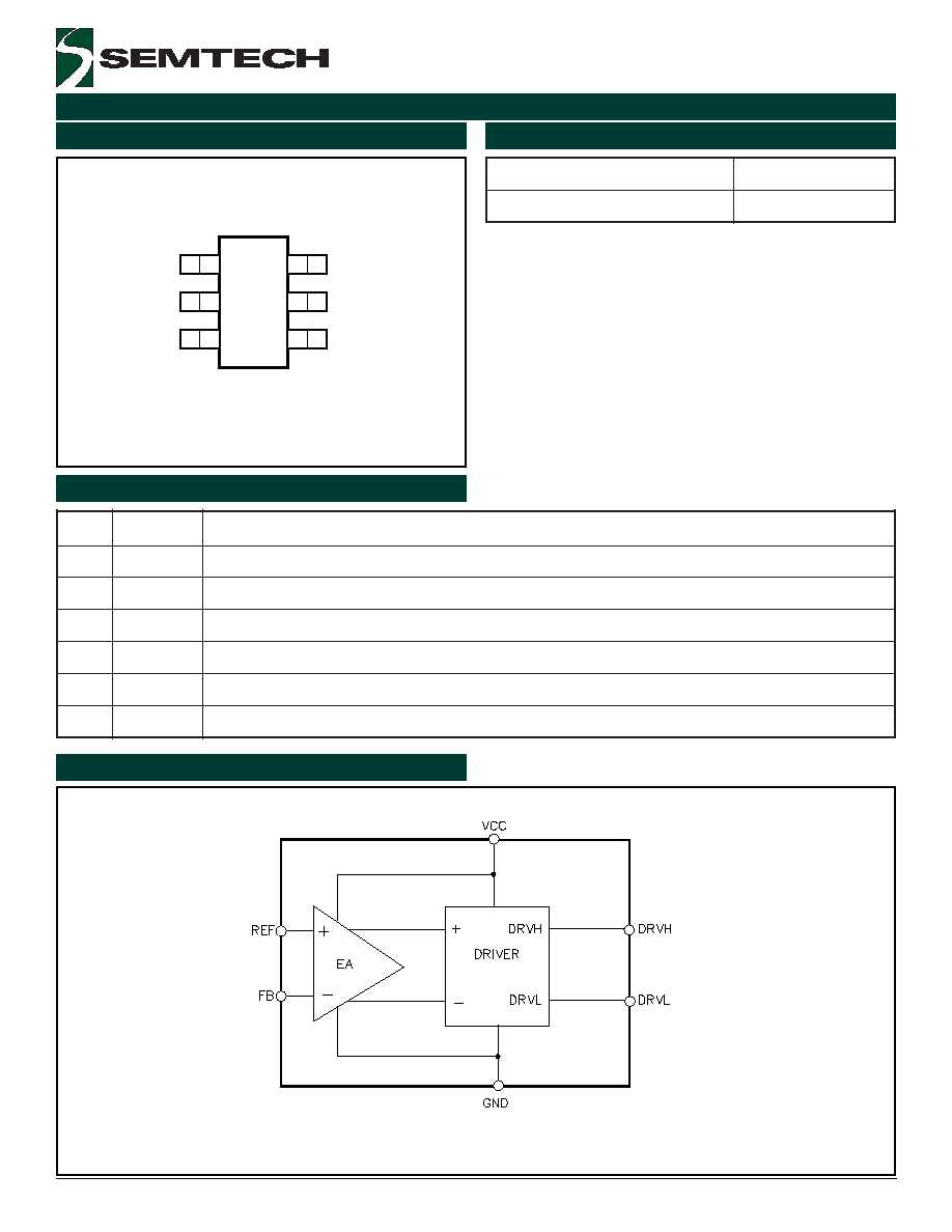
Pin Descriptions
Note:
(1) Only available in tape and reel packaging. A reel
contains 3000 devices.
r
e
b
m
u
N
t
r
a
P
e
g
a
k
c
a
P
R
T
K
S
I
6
1
1
1
C
S
)
1
(
L
6
3
2
-
T
O
S
Ordering Information
Pin Configuration
3
1
VCC
TOP VIEW
(SOT-23 6L)
5
FB
REF
6
DRVH
4
DRVL
2
GND
Block Diagram

4
2003 Semtech Corp.
www.semtech.com
POWER MANAGEMENT
SC1116
Application Information
Overview
The SC1116 linear controller is designed to meet the
JEDEC specifications for termination of DDR-SDRAM.
Double Data Rate (DDR) memory is clocked at the same
speed as older SDRAM (synchronous dynamic random
access memory), yet handles twice the amount of data
by using the rising and falling edge of the clock signal for
data transfers. Another difference is that DDR memory
requires 2.5V instead of 3.3V used by standard SDRAM.
The other feature that separates DDR memory from a
conventional type is employment of the V
TT
termination
voltage. Main requirements for the V
TT
are that it must
track variations of V
DDQ
and be able to supply (source)
current, and absorb (sink) current.
The SC1116 controller offers a low cost solution for DDR
termination voltage regulation by using external pass el-
ements (MOSFETs). Having the flexibility of choosing the
MOSFETs allows for optimization on the basis of cost/
size/performance of the specific application.
Test Circuit & Waveforms
The test circuit is shown below in Figure 1.
Note that V
REF
voltage is supplied externally to eliminate
inaccuracy caused by resistor divider.
Figure 1.
R EF
3
DRVL
4
VCC
1
FB
5
G ND
2
DRVH
6
U 1
SC1 116
C 3
0 .1uF
C 2
1 uF
C 4
4.7nF
C 5
4 .7nF
C 6
2 70 uF
R3
1 k
R4
1 k
Q 1
IR37 14
Q 2
IR37 14
V TT =1.25V typ
C 1
1 00 uF
2 2m
3 2m
2xIsin k
Isin k
Po wer
E lectron ic
Cu rrent
Su pp ly
Loa d
Pu lse loa d, dc=50%
Iso urce/ Isink
Pro be
V DDQ =2.5V
V cc=5V
V ref=1.2 5V
5
2003 Semtech Corp.
www.semtech.com
POWER MANAGEMENT
SC1116
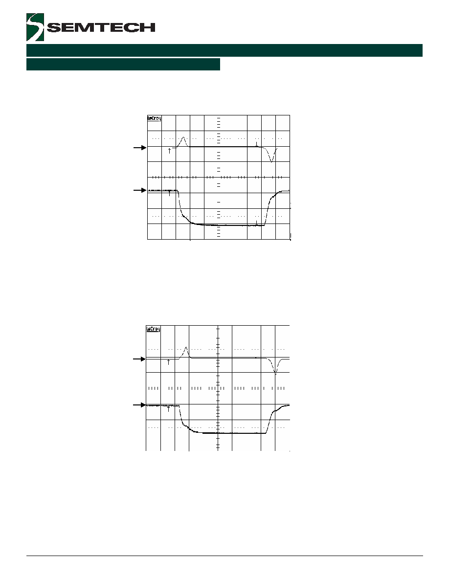
Test Waveforms
V
TT
100m
V
/
di
v
Time (50us/div)
I
S
O
URCE
/ I
SI
N
K
V
CC
= 5V
V
DDQ
= 2.5V
V
REF
= 1.25V
I
STEP
:
+2.3A
to - 2.2A
Slew Rate:
2.5 A/uS
V
TT
100m
V
/
di
v
I
S
O
URCE
/ I
SI
N
K
V
CC
= 5V
V
DDQ
= 2.5V
V
REF
= 1.25V
Time (50us/div)
I
STEP
:
+1.75A
to 1.75A
Slew Rate:
2.5 A/uS
V
TT
Transient Response