POWER MANAGEMENT
1
www.semtech.com
SC113X
Combination Switching Controller
and Low Dropout Regulator
Features
Applications
Revision 1, December 2000
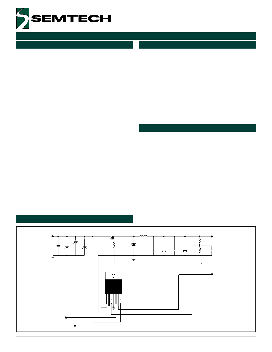
Typical Application Circuit
Description
The SC1131/2/3/4 incorporates a high current low
dropout linear regulator section together with a
switching voltage-mode controller. This unique combina-
tion is well suited for high current low voltage power sup-
ply applications such as the Intel Pentium
TM
P55, AMD
K6 and the Cyrix M2 processors. The SC113X was de-
signed to reduce the number of components required to
design a dual power supply for multivoltage processor
applications.
Switching Controller Section: The switching control
section is a voltage mode controller designed for high
current, low voltage power supply applications. Key
features include a temperature compensated voltage
reference, triangular oscillator and an internally
compensated transconductance error amplifier. The
switching controller operates at a fixed frequency of
200kHz, providing an optimum compromise between
size, efficiency and cost in the intended application
areas.
Linear Section: The linear portion is a high performance
positive voltage regulator designed for use in
applications requiring very low dropout performance
at 1.5, 3, 5 and 7.5 Amps. Additionally, the linear
section provides excellent regulation over variations due
to changes in line, load or temperature.
u
85% typical efficiency for switching section
u
Grounded tab
u
1.5, 2.5 or 3.3V @ 1% for linear section
u
Thermal shutdown
u
Internal short circuit protection (LDO)
u
7 pin TO-220 package
u
Microprocessor supplies
u
Modules supplies
u
1.3V to 3.5V power supplies
u
Dual power supplies from 5V source
Vout (SW)
5VIN
C1
0.1uF
C5
1000uF
+
C6
1000uF
+
BUK556
Q1
C4
1000uF
+
C3
1000uF
+
C2
1000uF
+
C7
1000uF
+
D1
L1
4uH
12V IN
SC1133
C9
+
1000uF
Vout (LIN)
C8
+
1000uF
R1
R2
C10
0.01uF
C11
0.1uF
R3
2.7
4
� 2000 Semtech Corp.
www.semtech.com
POWER MANAGEMENT
SC113X
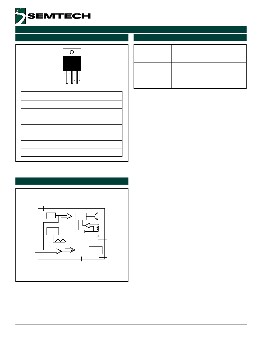
Block Diagram
ERROR
AMP
OSCILLATOR
+
-
Vo Sense
Vcc
GND
+
-
LEVEL SHIFT
AND DRIVE
DH
PGND
CURRENT LIMIT
Vout
THERMAL OVERLOAD
CONTROL
+
-
+
-
Vin
1.25V REF
(5)
(7)
(3)
(4)
(6)
(1)
(2)
Pin Configuration
Ordering Information
Note:
(1) Where XY denotes voltage options and lead con-
figurations. Available voltages (X) are: 1.5V, 2.5V and
3.3V. Available lead configurations (Y) are dual bend (DB),
single bend (SB) and straight leads (leave blank).
Sample part number: SC1133CT-2.5DB.
r
e
b
m
u
N
t
r
a
P
)
1
(
e
g
a
k
c
a
P
t
n
e
r
r
u
C
t
u
p
t
u
O
Y
X
-
T
C
1
3
1
1
C
S
0
2
2
-
O
T
A
5
.
1
Y
X
-
T
C
2
3
1
1
C
S
0
2
2
-
O
T
A
0
.
3
Y
X
-
T
C
3
3
1
1
C
S
0
2
2
-
O
T
A
0
.
5
Y
X
-
T
C
4
3
1
1
C
S
0
2
2
-
O
T
A
5
.
7
1 2 3 5 6 7
4
SC113X
#
n
i
P
e
m
a
N
n
i
P
n
o
it
c
n
u
F
1
H
D
t
u
p
t
u
O
r
e
v
ir
D
T
E
F
S
O
M
2
P
D
N
G
d
n
u
o
r
G
r
e
w
o
P
g
n
i
h
c
ti
w
S
3
o
V
E
S
N
E
S
)
r
e
h
c
ti
w
S
(
t
u
p
n
I
r
e
if
il
p
m
A
r
o
r
r
E
4
D
N
G
d
n
u
o
r
G
l
a
n
g
i
S
5
V
C
C
e
g
a
tl
o
V
t
u
p
n
I
V
2
1
+
6
V
T
U
O
V
T
U
O
)
n
o
it
c
e
S
r
a
r
e
n
i
L
(
7
V
N
I
e
g
a
tl
o
V
t
u
p
n
I
V
5
+
5
� 2000 Semtech Corp.
www.semtech.com
POWER MANAGEMENT
SC113X
PIN Descriptions
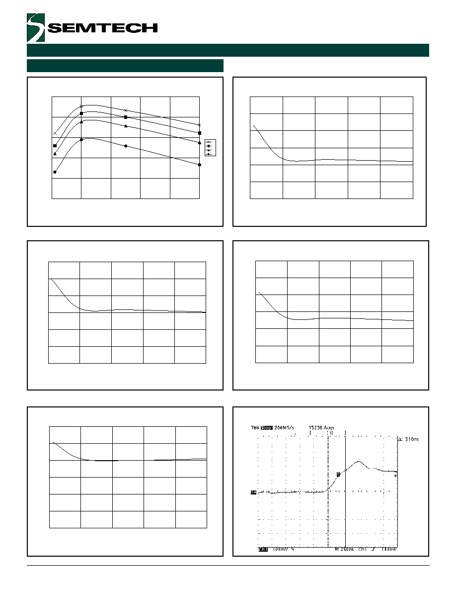
Typical Characteristics
70
75
80
85
90
95
0
2
4
6
8
10
3.3
2.9
2.5
1.8
SC113x Efficiency
%
Efficiency
Load Current (A)
Load Current (A)
-2.0
-1.5
-1.0
-0.5
0.0
0.5
1.0
0
2
4
6
8
10
-2.0
-1.5
-1.0
-0.5
0.0
0.5
1.0
0
2
4
6
8
10
-2.0
-1.5
-1.0
-0.5
0.0
0.5
1.0
0
2
4
6
8
10
-2.0
-1.5
-1.0
-0.5
0.0
0.5
1.0
0
2
4
6
8
10
% Load Regulation 3.3V, 0.3 to 10 Amps
% Load Regulation 2.9V, 0.3 to 10 Amps
Load Current (A)
Load Current (A)
% Load Regulation 2.3V, 0.2 to 10 Amps
% Load Regulation 1.8V, 0.2 to 10 Amps
Load Current (A)
Transient Load Current Rise 3.3V @ 10A