 | –≠–ª–µ–∫—Ç—Ä–æ–Ω–Ω—ã–π –∫–æ–º–ø–æ–Ω–µ–Ω—Ç: SC1157CS | –°–∫–∞—á–∞—Ç—å:  PDF PDF  ZIP ZIP |

SC1157
PROGRAMMABLE SYNCHRONOUS DC/DC
CONTROLLER FOR ADVANCED PROCESSORS
© 2000 SEMTECH CORP.
652 MITCHELL ROAD NEWBURY PARK CA 91320
Preliminary - August 7, 2000
1
Pentium is a registered trademark of Intel Corporation
BLOCK DIAGRAM
PIN CONFIGURATION
Top View
(16-Pin SOIC)
DESCRIPTION
The SC1157 is a low-cost, full featured, synchronous
voltage-mode controller designed for use in single
ended power supply applications where efficiency is of
primary concern. Synchronous operation allows for the
elimination of heat sinks in many applications. The
SC1157 is ideal for implementing DC/DC converters
needed to power advanced microprocessors such as
Pentium
Æ
ll (Klamath), in both single and multiple pro-
cessor configurations. Internal level-shift, high-side
drive circuitry, and preset shoot-thru control, allows for
use of inexpensive n-channel power switches.
SC1157 features include an integrated 4-bit V
ID
DAC,
temperature compensated voltage reference, triangle
wave oscillator, current limit comparator, frequency
shift over-current protection, and an internally compen-
sated error amplifier.
The SC1157 operates at a fixed 140KHz, providing an
optimum compromise between efficiency, external
component size, and cost.
FEATURES
∑
=
Low cost / full featured
∑
=
Synchronous operation
∑
=
4 Bit V
ID
DAC programmable output
(1% tolerance)
∑
=
Designed to meet Intel VRM8.2 (Pentium
Æ
II)
∑
=
1.5% Reference
APPLICATIONS
∑
=
PentiumÆ II Core Supply
∑
=
Multiple Microprocessor Supplies
∑
=
Voltage Regulator Modules (VRM)
∑
=
Programmable Power Supplies
∑
=
High Efficiency DC/DC Conversion
TEL:805-498-2111 FAX:805-498-3804 WEB:http://www.semtech.com
DEVICE
(1)
PACKAGE
(2)
TEMP. RANGE (T
J
)
SC1157CS.TR
SO-16NB
0 - 125∞C
ORDERING INFORMATION
Note:
(1) Only available in tape and reel packaging. A reel
contains 2500 devices.
(2) "NB" indicates 150 MIL body.
R
S
Q
+
-
70mV
+
-
+
-
ERROR
AMP
D/A
SHOOT-THRU
CONTROL
VCC
CS-
BSTH
DH
SHUTDOWN
CS+
BSTL
DL
PGND
VOSENSE
REF
VID2
VID1
VID0
GND
REF
CURRENT
LIMIT
LEVEL SHIFT AND
HIGH SIDE DRIVE
SYNCHRONOUS
MOSFET DRIVE
OSCILLATOR
VID3
SC1157
PROGRAMMABLE SYNCHRONOUS DC/DC
CONTROLLER FOR ADVANCED PROCESSORS
© 2000 SEMTECH CORP.
652 MITCHELL ROAD NEWBURY PARK CA 91320
Preliminary - August 7, 2000
2
NOTE:
(1) Specification refers to application circuit (Figure 1.).
(2) This device is ESD sensitive. Use of standard ESD handling precautions is required.
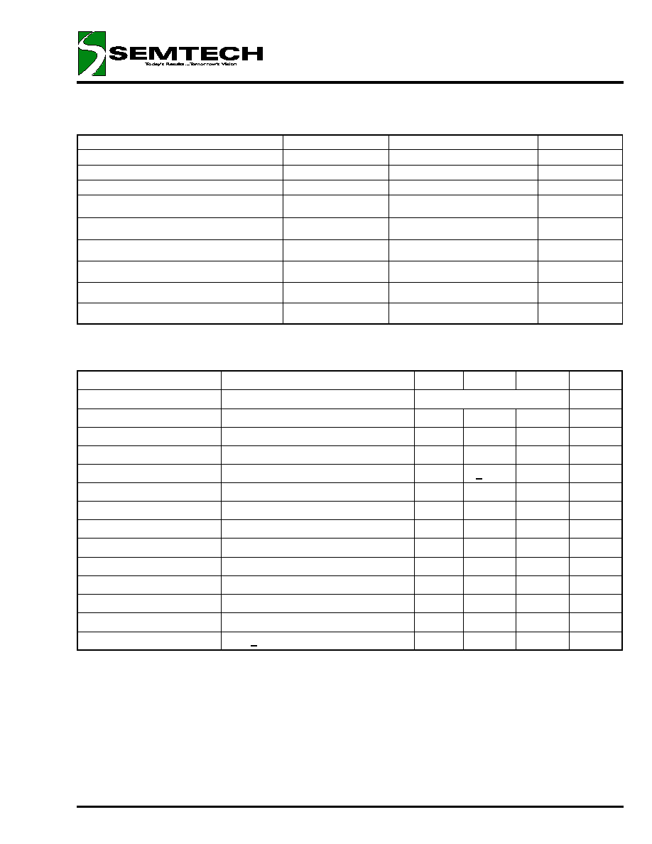
ELECTRICAL CHARACTERISTICS
Unless specified: V
CC
= 4.75V to 5.25V; GND = PGND = 0V; FB = V
O
; 0mV < (CS(+) - CS(-)) < 60mV; T
J
= 25
o
C
PARAMETER
CONDITIONS
MIN
TYP
MAX
UNITS
Output Voltage
See Table 1.
Supply Voltage
V
CC
4.5
7
V
Supply Current
V
CC
= 5.0
8
15
mA
Load Regulation
I
O
= 0.3A to 15A
(1)
1
%
Line Regulation
All VID codes
(1)
+
0.15
%
Gain (A
OL
)
V
OSENSE
to V
O
35
dB
Current Limit Voltage
60
70
80
mV
Oscillator Frequency
125
140
155
kHz
Buffered Reference Voltage
I
REF
=
1mA
1.25
V
Oscillator Max Duty Cycle
90
95
%
DH Sink/Source Current
BST
H
- DH = 4.5V, DH - PGND
H
= 3V
1
A
DL Sink/Source Current
BST
L
- DL = 4.5V, DL - PGND
L
= 3V
1
A
Dead Time
50
100
ns
VID Pin Source current
VIDx <
2.4V
30
100
uA
ABSOLUTE MAXIMUM RATINGS
Parameter
Symbol
Maximum
Units
V
CC
to GND
V
IN
-0.3 to 7
V
PGND to GND
± 1
V
BST to GND
-0.3 to 15
V
Thermal Resistance Junction to Case
JC
30
∞C/W
Thermal Resistance Junction to Ambient
JA
130
∞C/W
Operating Temperature Range
T
A
0 to 70
∞C
Storage Temperature Range
T
STG
-65 to +150
∞C
Lead Temperature (Soldering) 10 sec
T
LEAD
300
∞C
ESD Rating (Human Body Model)
ESD
1.5
kV

SC1157
PROGRAMMABLE SYNCHRONOUS DC/DC
CONTROLLER FOR ADVANCED PROCESSORS
© 2000 SEMTECH CORP.
652 MITCHELL ROAD NEWBURY PARK CA 91320
Preliminary - August 7, 2000
3
PIN CONFIGURATION
NOTE:
(1) All logic level inputs and outputs are open collector TTL compatible.
PIN DESCRIPTION
Pin #
Pin Name
Pin Function
1
GND
Small Signal Analog and Digital Ground
2
REF
Buffered Reference output
3
V
CC
Chip Supply Voltage
4
CS(-)
Current Sense Input (negative)
5
CS(+)
Current Sense Input (positive)
6
PGND
Power Ground for High and Low Side Drivers
7
DH
High Side Driver Output
8
DL
Low Side Driver Output
9
BSTL
Vcc for Low Side Driver (Boost)
10
BSTH
Vcc for High Side Driver (Boost)
11
SHUTDOWN
Logic Low shuts down the converter; High or open for normal operation.
12
VOSENSE
Top end of internal feedback chain
13
VID3
(1)
Programming Input (MSB)
14
VID2
(1)
Programming Input
15
VID1
(1)
Programming Input
16
VID0
(1)
Programming Input (LSB)

SC1157
PROGRAMMABLE SYNCHRONOUS DC/DC
CONTROLLER FOR ADVANCED PROCESSORS
© 2000 SEMTECH CORP.
652 MITCHELL ROAD NEWBURY PARK CA 91320
Preliminary - August 7, 2000
4
NOTE:
(1) All VID codes not specifically listed are invalid and cause shutdown exactly as if the shutdown pin had been
asserted.
THEORY OF OPERATION
The voltage at the VOSENSE pin is applied, through the internal precision resistor feedback chain, to the inverting
input of the error amplifier. The non-inverting input of the error amplifier is supplied with a DC voltage derived by
the DAC from the internal trimmed bandgap voltage reference. The output of the error amplifier is compared to the
triangular output of the internal oscillator to generate a fixed frequency, variable duty cycle pulse train. The internal
oscillator uses an on-chip capacitor and precision trimmed current sources to set the frequency to 100 kHz.
The generated pulse train is gated with the output of the current limit latch and the inhibit signal to produce a drive
signal for the upper FET. It is also inverted to produce a drive signal for the lower FET. These FET drive signals
are modified by the "shoot-through control" circuitry so that the top FET turn-on is delayed until the bottom FET has
turned off, and visa-versa.
The current limit latch is set (ending the upper FET drive pulse early) if the current limit comparator indicates an
overcurrent condition. The latch is reset at the start of each oscillator period.
OUTPUT VOLTAGE TABLE
Unless specified: V
CC
= 4.75V to 5.25V; GND = PGND = 0V; FB = V
O
; 0mV < (CS(+) - CS(-)) < 60mV;
T
J
= 0∞C to 85∞C
PARAMETER
CONDITIONS
VID
3210
MIN
TYP
MAX
UNITS
Output Voltage
(1)
I
O
= 2A in Application Circuit
1111
1.287
1.300
1.313
V
(Figure 1)
1110
1.337
1.350
1.364
1101
1.386
1.400
1.414
1100
1.436
1.450
1.465
1011
1.485
1.500
1.515
1010
1.535
1.550
1.566
1001
1.584
1.600
1.616
1000
1.634
1.650
1.667
0111
1.683
1.700
1.717
0110
1.733
1.750
1.768
0101
1.782
1.800
1.818
0100
1.832
1.850
1.869
0011
1.881
1.900
1.919
0010
1.931
1.950
1.970
0001
1.980
2.000
2.020
0000
2.030
2.050
2.070

SC1157
PROGRAMMABLE SYNCHRONOUS DC/DC
CONTROLLER FOR ADVANCED PROCESSORS
© 2000 SEMTECH CORP.
652 MITCHELL ROAD NEWBURY PARK CA 91320
Preliminary - August 7, 2000
5
OUTLINE DRAWING SO-16
LAND PATTERN SO-16
Jedec MS-012AC
ECN00-1243