Äîêóìåíòàöèÿ è îïèñàíèÿ www.docs.chipfind.ru
POWER MANAGEMENT
1
www.semtech.com
SC1175
Low Power Dual Synchronous DC/DC
Controller With Current Sharing Circuitry
Description
Features
Applications
Revision 7/31/2000
The SC1175 is a versatile 2 phase, synchronous, voltage mode
PWM controller that may be used in two distinct ways. First, the
SC1175 is ideal for applications where point of use output power
exceeds any single input power budget. Alternatively, the SC1175
can be used as a dual switcher. The SC1175 features a tempera-
ture compensated voltage reference, over current protection with
50% fold-back and internal level-shifted, high-side drive circuitry.
In current sharing configuration, the SC1175 can produce a single
output voltage from two separate voltage sources (which can be
different voltage levels) while maintaining current sharing between
the channels. Current sharing is programmable to allow loading
each input supply as required by the application.
In dual switcher configuration, two feedback paths are provided
for independent control of the separate outputs. The device will
provide a regulated output from flexibly configured inputs (3.3V,
5V, 12V), provided 5V is present for V
CC
. The two switchers are
180° out of phase to minimize input and output ripple.
u
300kHz fixed frequency operation
u
Soft Start and Enable function
u
Power Good output provided
u
Over current protection with 50% fold-back
u
Phase-shifted switchers minimize ripple
u
High efficiency operation, >90%
u
Programmable output(s) as low as 1.25V
u
Industrial temperature range
u
SOIC 20 pin package
Two Phase, Current Sharing Controller
u
Flexible, same or separate V
IN
u
Programmable current sharing
u
Combined current limit with fold-back
u
2 phases operating opposed for ripple reduction
u
Thermal distribution via multi-phase output
Two Independent PWM Controllers
u
Flexible, same or separate V
IN
u
Independent control for each channel
u
Independent and separate current limit
u
2 phases operating opposed for ripple reduction (if same
V
IN
used)
u
Graphics cards
u
DDR Memory
u
Peripheral add-in card
u
SSTL Termination
u
Dual-Phase power supply
u
Power supplies requiring two outputs
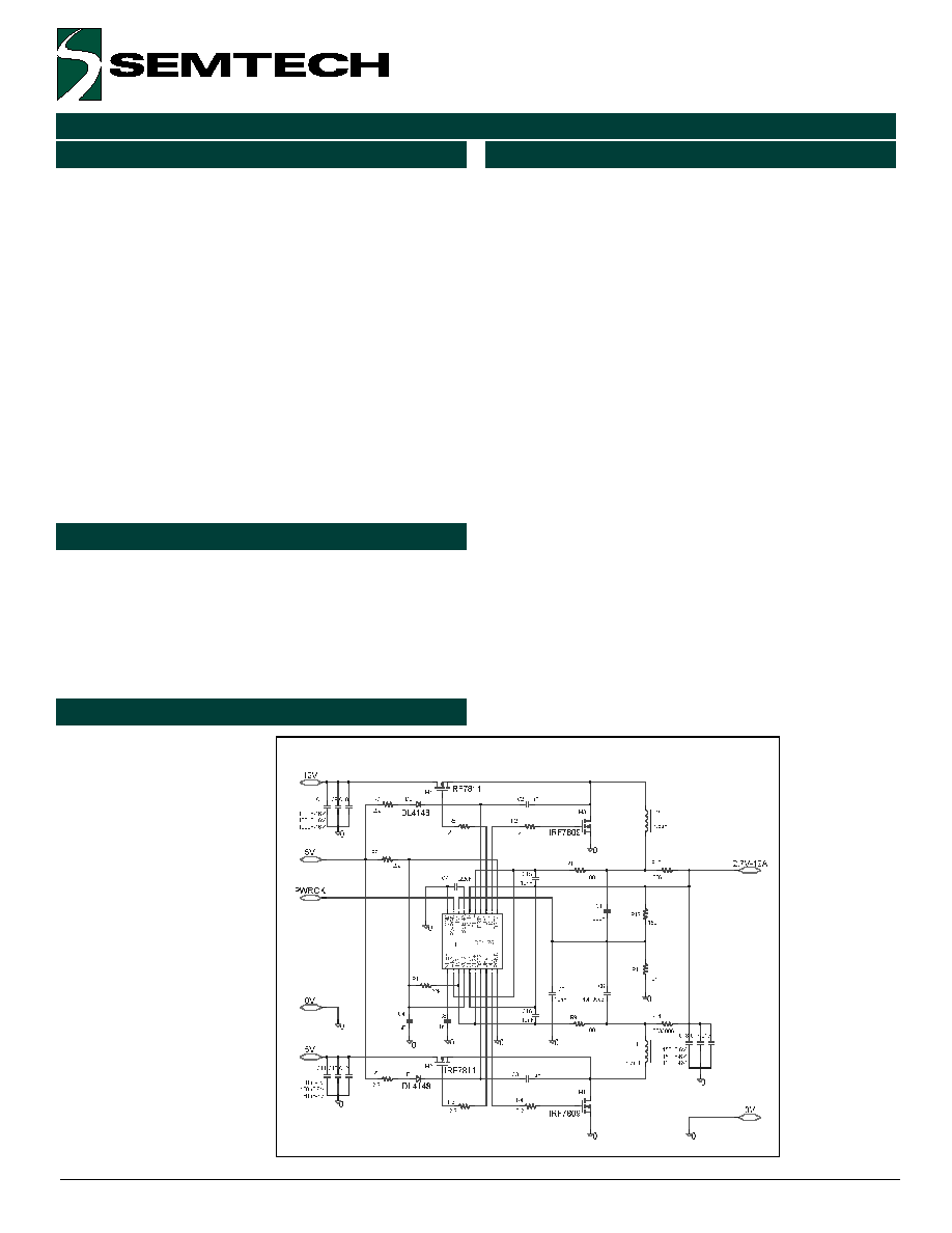
Typical Application Circuit
2 Channels with Current Sharing

2
ã 2000 Semtech Corp.
www.semtech.com
SC1175
POWER MANAGEMENT
Electrical Characteristics
R
E
T
E
M
A
R
A
P
S
N
O
I
T
I
D
N
O
C
N
I
M
P
Y
T
X
A
M
S
T
I
N
U
e
g
a
tl
o
V
t
u
p
t
u
O
I
O
A
2
=
)
1
(
V
,
T
U
O
V
5
7
.
2
o
t
t
e
s
5
6
.
2
5
7
.
2
5
8
.
2
V
e
g
a
tl
o
V
y
l
p
p
u
S
V
C
C
2
.
4
5
1
V
t
n
e
rr
u
C
y
l
p
p
u
S
V
C
C
0
.
5
=
0
1
A
m
e
c
n
e
r
e
f
e
R
-
5
7
3
2
.
1
1
±
5
2
.
1
-
5
2
6
2
.
1
1
±
V
n
o
it
a
l
u
g
e
R
d
a
o
L
I
O
A
5
1
o
t
A
3
.
0
=
)
1
(
1
%
n
o
it
a
l
u
g
e
R
e
n
i
L
e
c
n
e
r
e
f
e
R
V
5 < V
C
C
<
V
5
1
5
.
%
n
o
it
a
l
u
g
e
R
e
n
i
L
t
u
p
t
u
O
V
5 < V
N
I
<
V
5
1
5
.
%
A
(
n
i
a
G
L
O
)
V
E
S
N
E
S
O
V
o
t
O
5
3
B
d
e
g
a
tl
o
V
ti
m
i
L
t
n
e
rr
u
C
0
6
0
7
0
8
V
m
y
c
n
e
u
q
e
r
F
r
o
t
a
ll
i
c
s
O
0
7
2
0
0
3
0
3
3
z
H
k
e
l
c
y
C
y
t
u
D
x
a
M
r
o
t
a
ll
i
c
s
O
0
9
5
9
%
t
n
e
rr
u
C
k
n
i
S
H
D
V
5
.
3
=
D
N
G
P
-
H
D
1
A
t
n
e
rr
u
C
k
n
i
S
H
D
V
5
7
.
1
=
D
N
G
P
-
H
D
5
.
A
t
n
e
rr
u
C
e
c
r
u
o
S
H
D
V
0
.
5
=
H
D
-
H
T
S
B
1
A
t
n
e
rr
u
C
e
c
r
u
o
S
H
D
V
5
.
2
=
H
D
-
H
T
S
B
5
.
A
Unless Specified: V
CC
= 4.75 to 5.25V, GND = PGND = 0V, FB = V
O
, 0mV < (CS(+) - CS(-)) < 60mV , T
J
= 25°C
r
e
t
e
m
a
r
a
P
l
o
b
m
y
S
s
ti
m
i
L
s
ti
n
U
V
C
C
D
N
G
o
t
V
I
N
5
1
o
t
3
.
0
-
V
D
N
G
o
t
D
N
G
P
1
±
V
D
N
G
o
t
T
S
B
6
2
o
t
3
.
0
-
V
e
s
a
C
o
t
n
o
it
c
n
u
J
e
c
n
a
t
s
i
s
e
R
l
a
m
r
e
h
T
C
J
0
3
W
/
C
°
t
n
e
i
b
m
A
o
t
n
o
it
c
n
u
J
e
c
n
a
t
s
i
s
e
R
l
a
m
r
e
h
T
A
J
0
9
C
°
W
/
g
n
it
a
r
e
p
O
e
g
n
a
R
e
r
u
t
a
r
e
p
m
e
T
t
n
e
i
b
m
A
T
A
5
8
o
t
0
C
°
g
n
it
a
r
e
p
O
e
g
n
a
R
e
r
u
t
a
r
e
p
m
e
T
n
o
it
c
n
u
J
T
J
5
2
1
o
t
0
C
°
e
g
n
a
R
e
r
u
t
a
r
e
p
m
e
T
e
g
a
r
o
t
S
T
G
T
S
0
5
1
+
o
t
5
6
-
C
°
c
e
s
0
1
)
g
n
ir
e
d
l
o
S
(
e
r
u
t
a
r
e
p
m
e
T
d
a
e
L
T
D
A
E
L
0
0
3
C
°
q
q
Absolute Maximum Rating
3
ã 2000 Semtech Corp.
www.semtech.com
SC1175
POWER MANAGEMENT
Electrical Characteristics (Cont.)
R
E
T
E
M
A
R
A
P
S
N
O
I
T
I
D
N
O
C
N
I
M
P
Y
T
X
A
M
S
T
I
N
U
t
n
e
rr
u
C
k
n
i
S
L
D
V
5
.
3
=
D
N
G
P
-
L
D
1
A
t
n
e
rr
u
C
k
n
i
S
L
D
V
5
7
.
1
=
D
N
G
P
-
L
D
5
.
A
t
n
e
rr
u
C
e
c
r
u
o
S
L
D
V
5
=
L
D
-
L
T
S
B
1
A
t
n
e
rr
u
C
e
c
r
u
o
S
L
D
V
5
.
2
=
L
D
-
L
T
S
B
5
.
A
e
m
i
T
d
a
e
D
0
5
0
0
1
s
n
t
n
e
rr
u
C
e
g
r
a
h
C
tr
a
t
S
tf
o
S
)
2
(
5
2
A
µ
e
l
b
a
n
E
tr
a
t
S
tf
o
S
e
l
c
y
c
y
t
u
d
%
0
4
.
1
V
d
n
E
tr
a
t
S
tf
o
S
e
l
c
y
c
y
t
u
d
%
0
0
1
5
.
2
V
n
o
it
i
s
n
a
r
T
tr
a
t
S
tf
o
S
)
2
(
e
d
o
m
s
u
o
n
o
r
h
c
n
y
S
3
.
3
V
w
o
d
n
i
W
d
o
o
G
r
e
w
o
P
)
3
(
+ 0
1
V
%
T
U
O
t
n
e
rr
u
C
k
c
a
B
d
l
o
F
V
T
U
O
V
0
=
%
0
5
I
M
I
L
e
e
n
K
e
g
a
tl
o
V
k
c
a
B
d
l
o
F
=
I I
M
I
L
5
2
.
1
V
T
U
O
V
t
n
e
rr
u
C
s
a
i
B
t
u
p
n
I
2
N
I-
,
2
N
I
+
,
1
N
I-
1
A
µ
NOTES:
(1) Specification refers to application circuit.
(2) The soft start pin sources 25µA to an external capacitor. The converter operates in synchronous mode above the soft
start transition threshold and in asynchronous mode below it.
(3) Power good is an open collector pulled low when the output voltage is outside the ±10% window.
(4) This device is ESD sensitive. Use of standard ESD handling precautions is required.
Unless Specified: V
CC
= 4.75 to 5.25V, GND = PGND = 0V, FB = V
O
, 0mV < (CS(+) - CS(-)) < 60mV , T
J
= 25°C
4
ã 2000 Semtech Corp.
www.semtech.com
SC1175
POWER MANAGEMENT
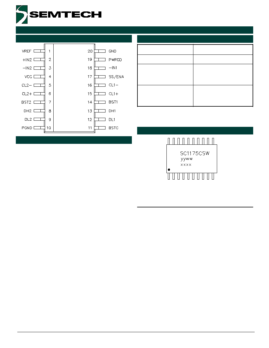
EXPANDED PIN DESCRIPTION
Pin 1: (VREF)
Internal 1.25V reference
Connected to the + input of the master channel error
amplifier.
Pin 2: (+IN)
+ Input of slave channel error amplifier.
Connected to 1.25V reference (Pin 1) for the two
independent channel configuration.
Pin 3, 18: (-IN2, -IN1)
- Inputs of close loop error amplifiers.
Works as a feedback inputs (For both modes).
Pin 4: (VCC)
VCC chip supply voltage.
15V maximum, 10mA typical.
Needs a 1µF ceramic multilayer decoupling capaci-
tor to GND (Pin 20).
Pin 5, 6,15, 16: (CL2-, CL2+, CL1+, CL1-)
Pins (-) and (+) of the current limit amplifiers for both
channels.
Connected to output current sense resistors. Com-
pares that sense voltage to internal 75mV reference.
Needs RC filter for noise rejection.
Pin 7, 14: (BST2, BST1)
BST signal. Supply for high side driver.
Can be connected to a high enough voltage source.
Usually connected to bootstrap circuit.
Pin 8, 13: (DH2, DH1)
DH signal (Drive High).
Gate drive for top MOSFETs.
Requires a small series resistor.
Pin 9, 12: (DL2, DL1)
DL signal (Drive Low).
Gate drive for bottom MOSFETs.
Requires a small series resistor.
Pin 10: (PGND)
Power GND. Return of gate drive currents.
Pin 11: (BSTC)
Supply for bottom MOSFETs gate drive.
Pin 17: (SS/ENA)
Soft start pin. Internal current source connected to
external capacitor.
Inhibits the chip if pulled down.
Pin 19: (PWRGD)
Power good signal.
Open collector signal .
Turns to 0 if output voltage is outside the power good
window.
Pin 20: (GND)
Analog GND.
Return of analog signals and bias of chip.
E
C
I
V
E
D
)
1
(
E
G
A
K
C
A
P
R
T
.
W
S
C
5
7
1
1
C
S
0
2
-
O
S
1
-
B
V
E
5
7
1
1
C
S
E
R
A
H
S
T
N
E
R
R
U
C
N
O
I
T
A
U
L
A
V
E
N
O
I
S
R
E
V
D
R
A
O
B
2
-
B
V
E
5
7
1
1
C
S
L
E
N
N
A
H
C
L
A
U
D
N
O
I
T
A
U
L
A
V
E
N
O
I
S
R
E
V
D
R
A
O
B
Notes:
(1) Only available in tape and reel packaging. A reel
contains 1000 devices
Pin Configuration
Ordering Information
Pin Descriptions
Marking Information
TOP
yyww = Datecode (Example: 9908)
xxxx = Semtech Lot # (Example: 90101)
5
ã 2000 Semtech Corp.
www.semtech.com
SC1175
POWER MANAGEMENT
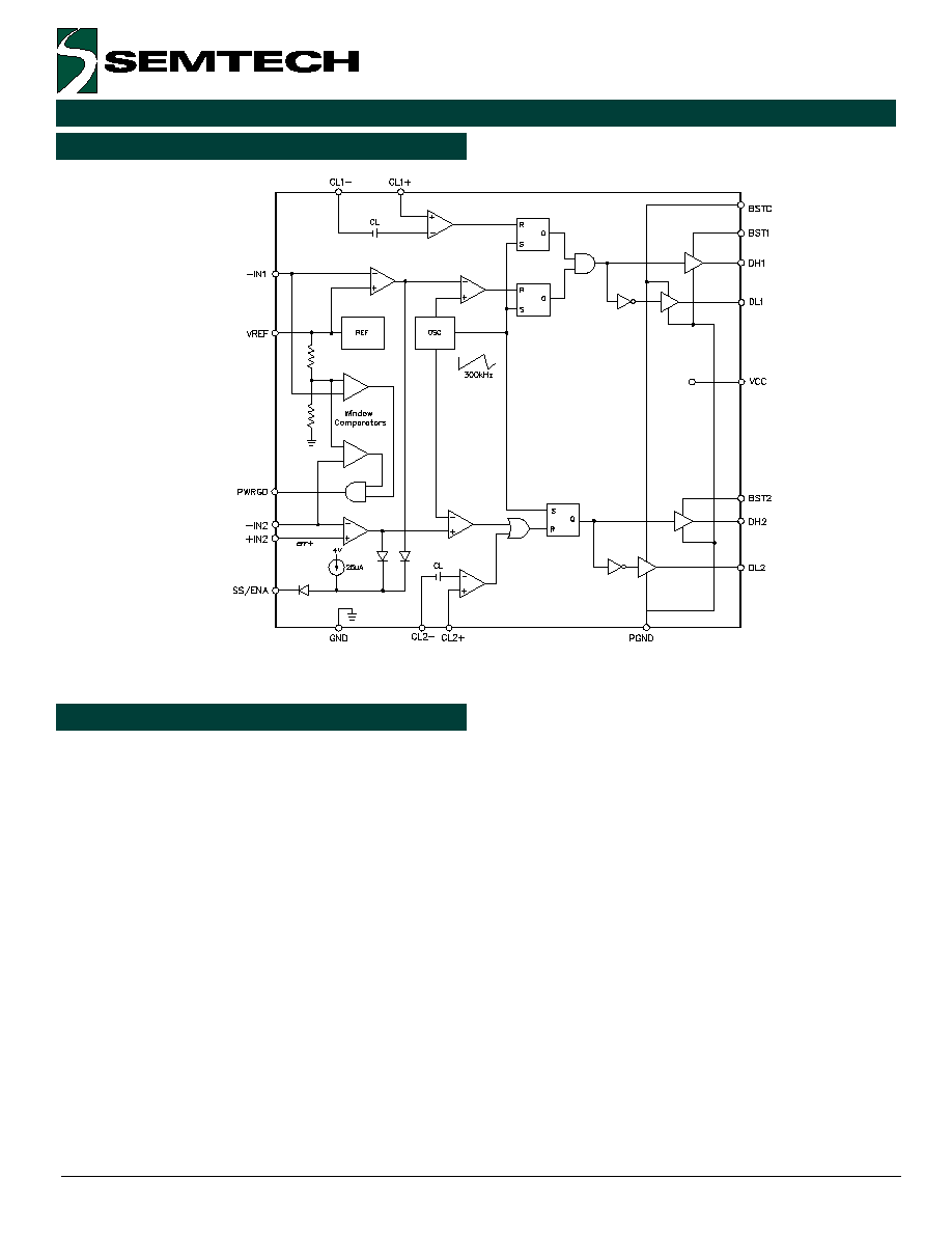
Applications Information
NOTES
(1) Block 1 (top) is the Master and Block 2 (bottom) is the Slave in current sharing configuration.
(2) For independant operation there is no Master or Slave.
Theory of Operation
Main Loop(s)
The SC1175 is a dual, voltage mode synchronous
Buck controller, the two separate channels are
identical and share only IC supply pins (Vcc and
GND), output driver ground (PGND) and pre-driver
supply voltage (BSTC). They also share a common
oscillator generating a sawtooth waveform for chan-
nel 1 and an inverted sawtooth for channel 2. Each
channel has its own current limit comparator. Chan-
nel 1 has the positive input of the error amplifier
internally connected to Vref. Channel 2 has both
inputs of the error amplifier uncommitted and avail-
able externally. This allows the SC1175 to operate in
two distinct modes.
a) Two independent channels with either com-
mon or different input voltages and different
output voltages. The two channels each have
their own voltage feedback path from their own
output. In this mode, the positive input of error
amplifier 2 is connected externally to Vref. If the
application uses a common input voltage, the
sawtooth phase shift between the channels
provides some measure of input ripple current
cancellation.
b) Two channels operating in current sharing
mode with common output voltage and either
common input voltage or different input voltages.
In this mode, channel 1 operates as a voltage
mode Buck controller, as before, but error amp 2
monitors and amplifies the difference in voltage
across the output current sense resistors of
channel 1 and channel 2 (Master and Slave) and
adjusts the Slave duty cycle to match output
currents. Because of finite gain and offsets in the
loop, the resistor ratio for perfect current match-
Block Diagram