POWER MANAGEMENT
1
www.semtech.com
SC431
Adjustable Shunt Regulator
Description
Features
Revision 7, May 2003
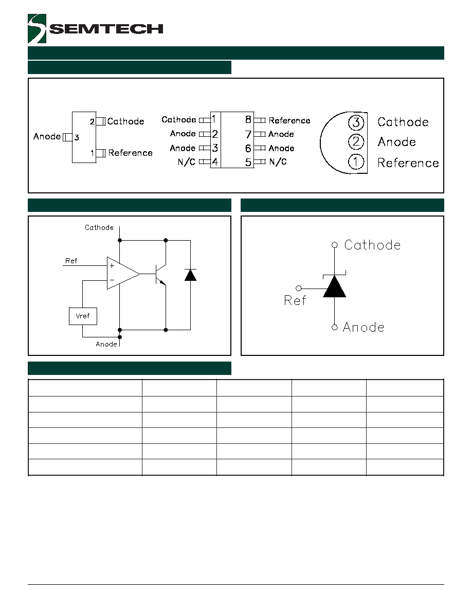
The SC431 is a three terminal adjustable shunt
regulator with thermal stability guaranteed over
temperature. The output voltage can be adjusted to any
value from 2.5V (V
REF
) to 30V with two external
resistors. The SC431 has a typical dynamic output
impedance of 0.25
. Active output circuitry provides a
very sharp turn on characteristic, making the SC431 an
excellent replacement for zener diodes.
The SC431 shunt regulator is available with four
voltage tolerances (0.5%, 1.0% and 2.0% over T
A
= -40
∞
C
to +85
∞
C and 0.5% over T
A
= -40
∞
C to +125
∞
C) and three
package options (SOT-23-3, SO-8 and TO-92). This
allows the designer the opportunity to select the
optimum combination of cost and performance for their
application.
Linear Regulators
Adjustable Supplies
Switching Power Supplies
Battery Operated Computers
Instrumentation
Computer Disk Drives
Wide operating current range 130µA to 150mA
Low dynamic output impedance 0.25
typ.
Trimmed bandgap design + 0.5%
Alternate for TL1431, TL431, LM431 & AS431
Industrial temperature range
Available in SOT-23-3, SO-8 and TO-92 packages
Notes:
1) Set V
OUT
according to the following equation:
1
R
I
2
R
1
R
1
V
V
REF
REF
OUT
+
+
=
2) Choose the value for R as follows:
∑
The maximum limit for R should be such that the
cathode current, I
Z
, is greater than the minimum
operating current (130µA) at V
IN(MIN)
.
∑
The minimum limit for R should be such that I
Z
does
not exceed 150mA under all load conditions, and the
instantaneous turn-on value for I
Z
does not exceed
200mA. Both of the following conditions must be met:
mA
200
V
R
(max)
IN
min
(to limit instantaneous turn-on I
Z
)
mA
150
I
V
V
R
(min)
OUT
OUT
(max)
IN
min
+
-
(to limit I
Z
under normal
operating conditions)
Applications
Typical Application Circuit
(1)(2)
2
2003 Semtech Corp.
www.semtech.com
POWER MANAGEMENT
SC431
Absolute Maximum Ratings
Electrical Characteristics
r
e
t
e
m
a
r
a
P
l
o
b
m
y
S
m
u
m
i
x
a
M
s
t
i
n
U
e
g
a
tl
o
V
e
d
o
h
t
a
C
V
Z
1
3
V
t
n
e
r
r
u
C
e
d
o
h
t
a
C
s
u
o
n
it
n
o
C
I
Z
0
5
1
A
m
t
n
e
r
r
u
C
t
u
p
n
I
e
c
n
e
r
e
f
e
R
I
F
E
R
0
1
A
m
T
t
a
n
o
it
a
p
i
s
s
i
D
r
e
w
o
P
A
C
∞
5
2
=
3
-
3
2
-
T
O
S
8
-
O
S
2
9
-
O
T
P
D
7
3
.
0
8
7
.
0
5
9
.
0
W
e
c
n
a
t
s
i
s
e
R
l
a
m
r
e
h
T
3
-
3
2
-
T
O
S
8
-
O
S
2
9
-
O
T
A
J
6
3
3
3
6
1
2
3
1
W
/
C
∞
e
g
n
a
R
e
r
u
t
a
r
e
p
m
e
T
t
n
e
i
b
m
A
g
n
it
a
r
e
p
O
2
-
x
C
1
3
4
C
S
,
1
-
x
C
1
3
4
C
S
,
5
.
-
x
C
1
3
4
C
S
Q
x
C
1
3
4
C
S
T
A
5
8
+
o
t
0
4
-
5
2
1
+
o
t
0
4
-
C
∞
e
g
n
a
R
e
r
u
t
a
r
e
p
m
e
T
n
o
it
c
n
u
J
g
n
it
a
r
e
p
O
T
J
0
5
1
+
o
t
0
4
-
C
∞
e
g
n
a
R
e
r
u
t
a
r
e
p
m
e
T
e
g
a
r
o
t
S
T
G
T
S
0
5
1
+
o
t
5
6
-
C
∞
s
d
n
o
c
e
s
0
1
)
g
n
ir
e
d
l
o
S
(
e
r
u
t
a
r
e
p
m
e
T
d
a
e
L
T
D
A
E
L
0
0
3
C
∞
)l
e
d
o
M
y
d
o
B
n
a
m
u
H
(
g
n
it
a
R
D
S
E
V
D
S
E
2
V
k
,
5
.
-
x
C
1
3
4
C
S
Q
x
C
1
3
4
C
S
1
-
x
C
1
3
4
C
S
r
e
t
e
m
a
r
a
P
l
o
b
m
y
S
n
o
i
t
i
d
n
o
C
n
i
M
p
y
T
x
a
M
n
i
M
p
y
T
x
a
M
s
t
i
n
U
e
g
a
tl
o
V
e
c
n
e
r
e
f
e
R
V
F
E
R
V
Z
V
=
F
E
R
I
,
Z
A
m
0
1
=
)
1
(
2
8
4
.
2
5
9
4
.
2
7
0
5
.
2
0
7
4
.
2
5
9
4
.
2
0
2
5
.
2
V
V
F
E
R
n
o
it
a
i
v
e
D
p
m
e
T
V
V
E
D
V
Z
V
=
F
E
R
, I
Z
A
m
0
1
=
)
1
(
8
7
1
8
5
2
V
m
n
i
e
g
n
a
h
C
f
o
o
it
a
R
I
Z
,
A
m
0
1
=
V
Z
V
o
t
V
0
1
=
F
E
R
5
.
0
-
7
.
2
-
5
.
0
-
7
.
2
-
V
/
V
m
V
F
E
R
V
n
i
e
g
n
a
h
C
o
t
Z
I
Z
,
A
m
0
1
=
V
Z
V
0
1
o
t
V
0
3
=
0
.
1
-
0
.
2
-
0
.
1
-
0
.
2
-
t
u
p
n
I
e
c
n
e
r
e
f
e
R
t
n
e
r
r
u
C
I
F
E
R
k
0
1
=
1
R
=
2
R
,
,
I
Z
A
m
0
1
=
)
2
(
5
.
0
4
5
.
0
4
A
µ
I
F
E
R
e
r
u
t
a
r
e
p
m
e
T
n
o
it
a
i
v
e
D
I
)
V
E
D
(
F
E
R
k
0
1
=
1
R
=
2
R
,
,
I
Z
A
m
0
1
=
)
2
(
4
.
0
2
.
1
4
.
0
2
.
1
A
µ
e
d
o
h
t
a
C
e
t
a
t
S
-
ff
O
t
n
e
r
r
u
C
I
)
F
F
O
(
Z
V
F
E
R
V
,
V
0
=
Z
V
0
3
=
)
3
(
4
0
.
0
0
5
.
0
4
0
.
0
0
5
.
0
A
µ
t
u
p
t
u
O
c
i
m
a
n
y
D
e
c
n
a
d
e
p
m
I
r
Z
V
,
z
H
k
1
<
f
Z
V
=
F
E
R
I
Z
A
m
0
0
1
o
t
A
µ
0
3
1
=
)
1
(
5
2
.
0
0
5
.
0
5
2
.
0
0
5
.
0
g
n
it
a
r
e
p
O
m
u
m
i
n
i
M
t
n
e
r
r
u
C
I
)
N
I
M
(
Z
V
Z
V
=
F
E
R
)
1
(
0
3
1
0
3
1
A
µ
Z
REF
V
V
Exceeding the specifications below may result in permanent damage to the device, or device malfunction. Operation outside of the parameters
specified in the Electrical Characteristics section is not implied.
Unless specified:T
A
= 25∞C. Values in bold apply over full operating ambient temperature range.
3
2003 Semtech Corp.
www.semtech.com
POWER MANAGEMENT
SC431
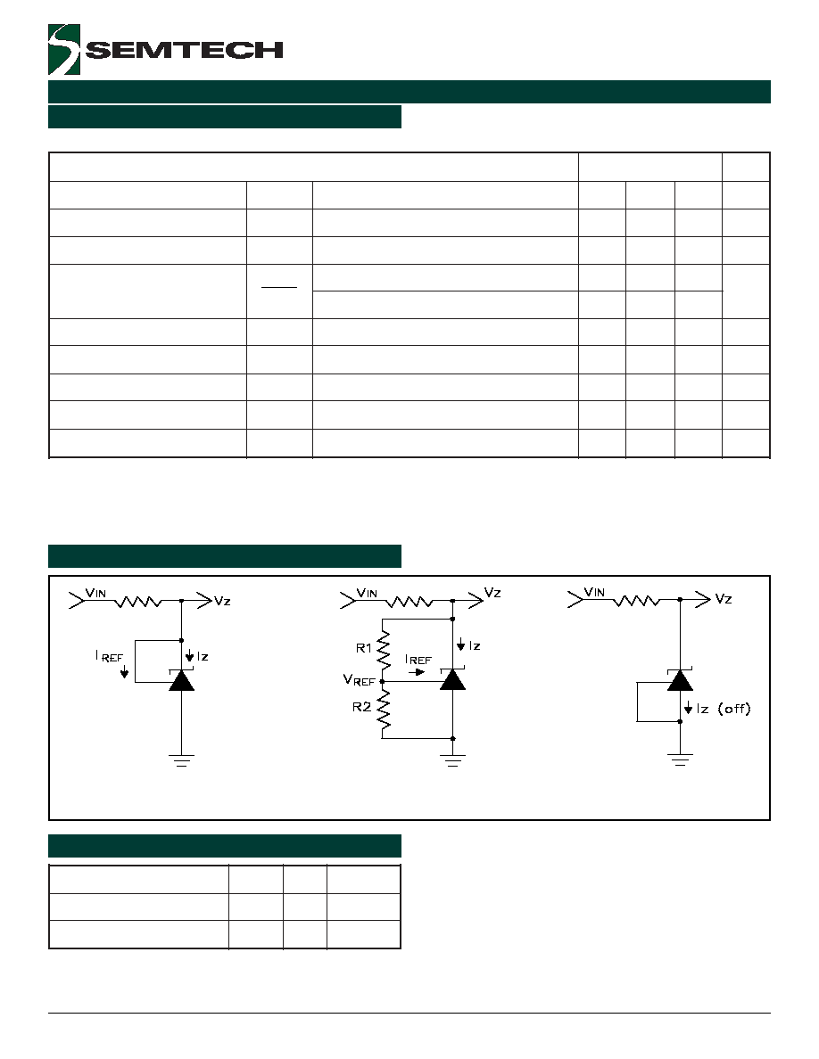
Test Circuit 3
Off-State
Test Circuit 2
V
Z
> V
REF
Test Circuit 1
V
Z
= V
REF
Electrical Characteristics (Cont.)
2
-
x
C
1
3
4
C
S
r
e
t
e
m
a
r
a
P
l
o
b
m
y
S
n
o
i
t
i
d
n
o
C
n
i
M
p
y
T
x
a
M
s
t
i
n
U
e
g
a
tl
o
V
e
c
n
e
r
e
f
e
R
V
F
E
R
V
Z
V
=
F
E
R
I
,
Z
A
m
0
1
=
)
1
(
5
4
4
.
2
5
9
4
.
2
5
4
5
.
2
V
V
F
E
R
n
o
it
a
i
v
e
D
p
m
e
T
V
V
E
D
V
Z
V
=
F
E
R
, I
Z
A
m
0
1
=
)
1
(
5
1
0
3
V
m
V
n
i
e
g
n
a
h
C
f
o
o
it
a
R
F
E
R
o
t
I
Z
,
A
m
0
1
=
V
Z
V
o
t
V
0
1
=
F
E
R
5
.
0
-
7
.
2
-
V
/
V
m
V
n
i
e
g
n
a
h
C
Z
I
Z
,
A
m
0
1
=
V
Z
V
0
1
o
t
V
0
3
=
0
.
1
-
0
.
2
-
t
n
e
r
r
u
C
t
u
p
n
I
e
c
n
e
r
e
f
e
R
I
F
E
R
k
0
1
=
1
R
=
2
R
,
I
,
Z
A
m
0
1
=
)
2
(
5
.
0
4
A
µ
I
F
E
R
n
o
it
a
i
v
e
D
e
r
u
t
a
r
e
p
m
e
T
I
)
V
E
D
(
F
E
R
k
0
1
=
1
R
=
2
R
,
, I
Z
A
m
0
1
=
)
2
(
4
.
0
2
.
1
A
µ
t
n
e
r
r
u
C
e
d
o
h
t
a
C
e
t
a
t
S
-
ff
O
I
)
F
F
O
(
Z
V
F
E
R
V
,
V
0
=
Z
V
0
3
=
)
3
(
4
0
.
0
0
5
.
0
A
µ
e
c
n
a
d
e
p
m
I
t
u
p
t
u
O
c
i
m
a
n
y
D
r
Z
V
,
z
H
k
1
<
f
Z
V
=
F
E
R
I
,
Z
A
m
0
0
1
o
t
A
µ
0
3
1
=
)
1
(
5
2
.
0
0
5
.
0
t
n
e
r
r
u
C
g
n
it
a
r
e
p
O
m
u
m
i
n
i
M
I
)
N
I
M
(
Z
V
Z
V
=
F
E
R
)
1
(
0
3
1
A
µ
Z
REF
V
V
Unless specified:T
A
= 25∞C. Values in bold apply over full operating ambient temperature range.
Notes:
(1) See Test Circuit 1 below.
(2) See Test Circuit 2 below.
(3) See Test Circuit 3 below.
n
i
M
x
a
M
l
o
b
m
y
S
V
,
e
g
a
tl
o
V
e
d
o
h
t
a
C
Z
V
F
E
R
0
3
V
I
,t
n
e
r
r
u
C
e
d
o
h
t
a
C
Z
0
3
1
.
0
0
5
1
A
m
Test Circuits
Recommended Operating Conditions

6
2003 Semtech Corp.
www.semtech.com
POWER MANAGEMENT
SC431
-300
-200
-100
0
100
200
300
-2
-1
0
1
2
3
V
Z
(V)
I
Z
(
A)
V
Z
= V
REF
T
A
= 25
o
C
-150
-100
-50
0
50
100
150
-2
-1
0
1
2
3
V
Z
(V)
I
Z
(mA)
V
Z
= V
REF
T
A
= 25
o
C
0
0.1
0.2
0.3
0.4
0.5
-50
-25
0
25
50
75
100
125
150
T
J
(∞C)
V
RE
F
/
V
Z
(-mV
/
V
)
I
Z
= 10mA
V
Z
= 3V to 30V
2.485
2.490
2.495
2.500
2.505
2.510
2.515
-50
-25
0
25
50
75
100
125
150
T
J
(∞C)
V
REF
(V)
V
Z
= V
REF
I
Z
= 10mA
0
20
40
60
80
100
-50
-25
0
25
50
75
100
125
150
T
J
(∞C)
I
REF
(nA)
I
Z
= 10mA
R1 = 10k
R2 =
0.001
0.01
0.1
1
10
100
-50
-25
0
25
50
75
100
125
150
T
J
(∞C)
I
Z
(
o
ff)
V
Z
= 30V
V
REF
= 0V
Cathode Current vs.
Cathode Voltage
Cathode Current vs.
Cathode Voltage
Reference Voltage vs.
Junction Temperature
Reference Input Current vs.
Junction Temperature
Ratio of Delta Reference Voltage to Delta Cathode
Voltage vs. Junction Temperature
Off-State Cathode Current
vs. Junction Temperature
Typical Characteristics
7
2003 Semtech Corp.
www.semtech.com
POWER MANAGEMENT
SC431
0.01
0.1
1
10
100
1.0E+03
1.0E+04
1.0E+05
1.0E+06
1.0E+07
f (Hz)
r
Z
(
)
I
Z
= 10mA
T
A
= 25∞C
-20
-10
0
10
20
30
40
50
60
70
80
1.0E+02
1.0E+03
1.0E+04
1.0E+05
1.0E+06
f (Hz)
A
V
(dB)
-630
-585
-540
-495
-450
-405
-360
-315
-270
-225
-180
Phase Shift (deg)
I
Z
= 10mA
T
A
= 25∞C
Small-Signal Gain and Phase Shift
vs. Frequency
Reference Impedance
vs. Frequency
Typical Characteristics (Cont.)
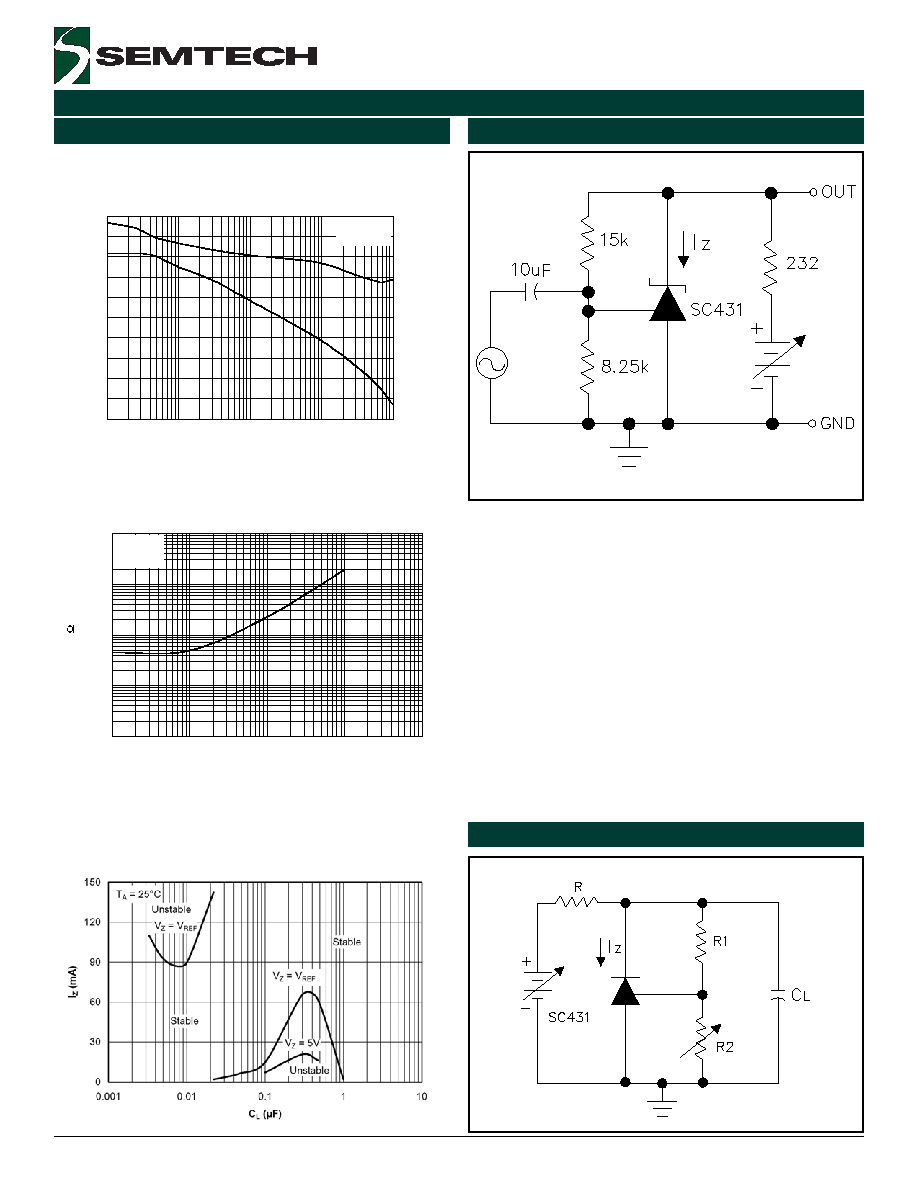
Test Circuit - Small-Signal Gain and Phase
Test Circuit - Stability
Stability Boundary Condition For Shunt Regulation
vs. Cathode Current and Load Capacitance
9
2003 Semtech Corp.
www.semtech.com
POWER MANAGEMENT
SC431
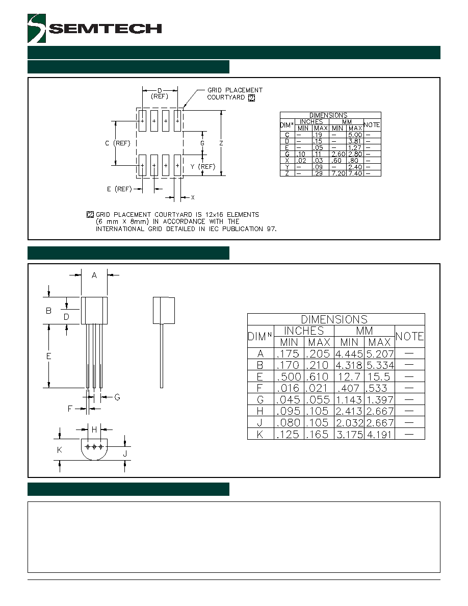
Land Pattern - SO-8
Semtech Corporation
Power Management Products Division
200 Flynn Road, Camarillo, CA 93012
Phone: (805)498-2111 FAX (805)498-3804
Contact Information
Outline Drawing - TO-92