ChipFind - документация

Электронный компонент: SC4505MLTRT

Скачать:  PDF   ZIP
1
www.semtech.com
SC4505
High Efficiency Boost Converter
for Backlight/Flash LED Driver
POWER MANAGEMENT
Description
Features
Applications
White LED power supplies
Flat screen LCD bias supplies
TFT bias supplies
Dual panel Handset/Liquid Crystal Display Monitor
Portable media players
Digital video cameras
Digital still cameras
The SC4505 is a high-frequency PWM current-mode step-
up switching regulator with an integrated 2A power tran-
sistor. Its high switching frequency (1MHz) allows the use
of tiny surface-mount external passive components. The
internal switch is rated at 36V which makes the con-
verter ideal for multiple LED series operation with opti-
mal current matching. Two programmable independent
current source structure allows dual panel LED backlight
and flash operation.
The operating frequency of the SC4505 is set at 1MHz.
The selected operating frequency gives the SC4505 de-
sign flexibility for size, cost and efficiency optimization.
The SC4505 is available in thermally enhanced 16-pin
MLPQ package (3x3x0.9mm) with embedded over tem-
perature protection.
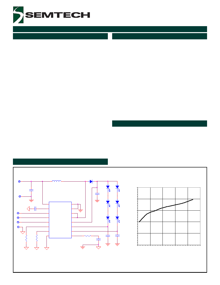
Typical Application Circuit
Two independent current sources for dual LED strands
with optimal current/light matching. Backlight up to
75mA, Flash up to 125mA
Wide input range from 2.6V to 12V
Adaptive output voltage up to 28V with OVP protec-
tion against open circuit conditions
Low shutdown current (<1
A )
Internal Flash/Torch mode with flash timeout to pro-
tect LEDs
1MHz Fixed Frequency Current-Mode Control
Internal 2A current limit for driving large numbers of
LEDs
Supports PWM Dimming from 50Hz to 50kHz
Internal undervoltage lockout
Small, low profile, thermally enhanced 16-MLPQ pack-
age is fully WEEE and RoHS compliant
Revision: January 17, 2006
Figure 1. SC4505 Application Circuit for Backlight and Flashlight LED Driver
All Capacitors are Ceramic.
PGND
C5
12n
0
SC4505
1
2
3
4
5
6
7
8
9
10
11
12
13
14
15
16
PGND
PGND
SW
SW
VO
IO2
IO1
COMP
AGND
IO2SET
IO1SET
EN_BL
EN_FL
FL_TRB
FTO
VIN
D5
LED
D4
LED
0
C4
12n
LED: SML-LX0603UWD
D2
LED
D7
LED
VIN: 2.6V ~ 6.0V
0
RO1SET
6.98k
0
D1
10BQ015
2
1
C1
2.2uF
EN_FL
Analog
Ground
C6
12n
C3
0.33uF
EN_BL
Power
Ground
AGND
0
L1
IHLP-2525CZ-01-1R5-M-01
0
R1
1.47k
D6
LED
D3
LED
FL_TRB
RO2SET
1.54k
C2
2.2u
Boost Converter Efficiency vs Input Voltage
(2 String of 3 LEDs @30mA)
77
79
81
83
85
87
2.5
3
3.5
4
4.5
5
Input Voltage (V)
E
f
f
i
ci
en
cy
(
%
)
2
2006 Semtech Corp.
www.semtech.com
SC4505
POWER MANAGEMENT
Absolute Maximum Rating
Electrical Characteristics
r
e
t
e
m
a
r
a
P
l
o
b
m
y
S
p
y
T
s
t
i
n
U
e
g
a
tl
o
V
y
l
p
p
u
S
V
N
I
0
2
o
t
3
.
0
-
V
e
g
a
tl
o
V
e
c
r
u
o
S
t
n
e
r
r
u
C
,
e
g
a
tl
o
V
t
u
p
t
u
O
,
e
g
a
tl
o
V
W
S
V
W
S
V
,
O
V
,
1
O
I
V
,
2
O
I
6
3
o
t
3
.
0
-
V
I
T
E
S
0
e
g
a
tl
o
V
V
,
T
E
S
1
O
I
V
T
E
S
2
O
I
2
o
t
3
.
0
-
V
e
g
a
tl
o
V
O
T
F
V
O
T
F
V
o
t
3
.
0
-
N
I
3
.
0
+
V
e
g
a
tl
o
V
B
R
T
_
L
F
,
L
F
_
N
E
,
L
B
_
N
E
V
L
B
_
N
E
V
,
L
F
_
N
E
V
B
R
T
_
L
F
V
o
t
3
.
0
-
N
I
3
.
0
+
V
t
n
e
i
b
m
A
o
t
n
o
it
c
n
u
J
e
c
n
a
t
s
i
s
e
R
l
a
m
r
e
h
T
A
J
5
.
3
3
W
/
C
e
r
u
t
a
r
e
p
m
e
T
n
o
it
c
n
u
J
m
u
m
i
x
a
M
T
J
0
5
1
C
e
g
n
a
R
e
r
u
t
a
r
e
p
m
e
T
e
g
a
r
o
t
S
T
G
T
S
0
5
1
+
o
t
5
6
-
C
s
0
3
o
t
s
0
1
)
g
n
ir
e
d
l
o
S
(
w
o
lf
e
R
R
I
T
D
A
E
L
0
6
2
C
)l
e
d
o
M
y
d
o
B
n
a
m
u
H
(
g
n
it
a
R
D
S
E
D
S
E
1
V
k
Unless specified: V
IN
= 3.6V, -40C < T
A
= T
J
< 85C, R
O1SET
=6.98K
,
R
O2SET
=1.54K
Exceeding the specifications below may result in permanent damage to the device, or device malfunction. Operation outside of the parameters specified
in the Electrical Characteristics section is not implied. Exposure to Absolute Maximum rated conditions for extended periods of time may affect device
reliability.
r
e
t
e
m
a
r
a
P
s
n
o
i
t
i
d
n
o
C
t
s
e
T
n
i
M
p
y
T
x
a
M
t
i
n
U
V
e
g
a
tl
o
V
t
u
p
n
I
y
l
p
p
u
S
N
I
6
.
2
2
1
V
d
l
o
h
s
e
r
h
T
O
L
V
U
V
N
I
g
n
i
s
ir
5
4
.
2
9
5
.
2
V
s
i
s
e
r
e
t
s
y
H
O
L
V
U
0
5
V
m
V
N
I
t
n
e
r
r
u
C
y
l
p
p
u
S
g
n
i
h
c
ti
w
s
t
o
N
7
.
1
A
m
V
N
I
n
w
o
d
t
u
h
S
n
i
t
n
e
r
r
u
C
y
l
p
p
u
S
0
=
L
B
_
N
E
=
B
R
T
_
L
F
=
L
F
_
N
E
0
.
1
A
y
c
n
e
u
q
e
r
F
g
n
i
h
c
ti
w
S
T
J
C
5
2
=
8
.
0
1
2
.
1
z
H
M
e
l
c
y
C
y
t
u
D
m
u
m
i
x
a
M
5
8
0
9
%
e
l
c
y
C
y
t
u
D
m
u
m
i
n
i
M
0
%
ti
m
i
L
t
n
e
r
r
u
C
h
c
ti
w
S
5
7
.
1
5
2
.
2
A
t
n
e
r
r
u
C
e
g
a
k
a
e
L
h
c
ti
w
S
V
W
S
V
5
=
1
0
.
0
1
A
e
g
a
tl
o
V
n
o
it
a
r
u
t
a
S
h
c
ti
w
S
I
W
S
A
1
=
0
0
3
V
m
L
B
_
N
E
,
B
R
T
_
L
F
,
L
F
_
N
E
e
g
a
tl
o
V
h
g
i
H
V
N
I
V
7
.
4
o
t
V
6
.
2
=
2
V
L
B
_
N
E
,
B
R
T
_
L
F
,
L
F
_
N
E
e
g
a
tl
o
V
w
o
L
V
N
I
V
7
.
4
o
t
V
6
.
2
=
4
.
0
V
3
2006 Semtech Corp.
www.semtech.com
SC4505
POWER MANAGEMENT
Electrical Characteristics (Cont.)
Unless specified: V
IN
= 3.6V, -40C < T
A
= T
J
< 85C, R
O1SET
=6.98K
,
R
O2SET
=1.54K
Note 1: Guaranteed by Design
r
e
t
e
m
a
r
a
P
s
n
o
i
t
i
d
n
o
C
t
s
e
T
n
i
M
p
y
T
x
a
M
t
i
n
U
L
B
_
N
E
,
B
R
T
_
L
F
,
L
F
_
N
E
t
n
e
r
r
u
C
t
u
p
n
I
V
L
F
_
N
E
V
7
.
4
o
t
V
0
=
1
0
.
0
1
A
g
n
i
m
m
i
D
M
W
P
L
B
_
N
E
y
c
n
e
u
q
e
r
F
l
o
r
t
n
o
C
1
e
t
o
N
0
5
K
0
5
z
H
g
n
i
m
m
i
D
M
W
P
L
B
_
N
E
e
l
c
y
C
y
t
u
D
l
o
r
t
n
o
C
1
e
t
o
N
0
0
0
1
%
t
n
e
r
r
u
C
g
n
i
c
r
u
o
S
O
T
F
1
=
B
R
T
_
L
F
=
L
F
_
N
E
2
.
1
A
e
g
a
tl
o
V
d
l
o
h
s
e
r
h
T
p
ir
T
O
T
F
5
2
.
1
V
t
n
e
r
r
u
C
n
w
o
D
ll
u
P
O
T
F
0
=
B
R
T
_
L
F
,
1
=
L
F
_
N
E
6
.
2
A
m
n
o
it
c
e
t
o
r
P
e
g
a
tl
o
v
r
e
v
O
8
2
V
e
r
u
t
a
r
e
p
m
e
T
n
w
o
d
t
u
h
S
l
a
m
r
e
h
T
5
5
1
C
s
i
s
e
r
e
t
s
y
H
n
w
o
d
t
u
h
S
l
a
m
r
e
h
T
0
1
C
y
c
a
r
u
c
c
A
t
n
e
r
r
u
C
t
h
g
il
k
c
a
B
I
(
1
O
)
1
=
L
B
_
N
E
T
J
R
,
C
5
2
=
T
E
S
1
O
K
8
9
.
6
=
9
1
0
2
1
2
A
m
I
(
t
n
e
r
r
u
C
t
h
g
il
k
c
a
B
x
a
M
1
O
)
5
7
A
m
I
(
y
c
a
r
u
c
c
A
t
n
e
r
r
u
C
h
s
a
l
F
2
O
)
1
=
B
R
T
_
L
F
=
L
F
_
N
E
T
J
R
,
C
5
2
=
T
E
S
2
O
K
4
5
.
1
=
2
9
0
0
1
8
0
1
A
m
I
(
t
n
e
r
r
u
C
h
s
a
l
F
x
a
M
2
O
)
5
2
1
A
m
I
(
t
n
e
r
r
u
C
t
u
p
t
u
O
h
c
r
o
T
2
O
)
0
=
B
R
T
_
L
F
,
1
=
L
F
_
N
E
T
J
R
,
C
5
2
=
T
E
S
2
O
K
4
5
.
1
=
8
1
A
m
I
1
O
t
n
e
r
r
u
C
e
g
a
k
a
e
L
ff
O
V
1
O
I
V
2
=
1
.
0
A
I
2
O
t
n
e
r
r
u
C
e
g
a
k
a
e
L
ff
O
V
2
O
I
V
2
=
1
.
0
A
V
O
tl
u
a
F
e
g
a
tl
o
v
r
e
v
O
n
i
n
w
o
d
ll
u
P
7
K
4
2006 Semtech Corp.
www.semtech.com
SC4505
POWER MANAGEMENT
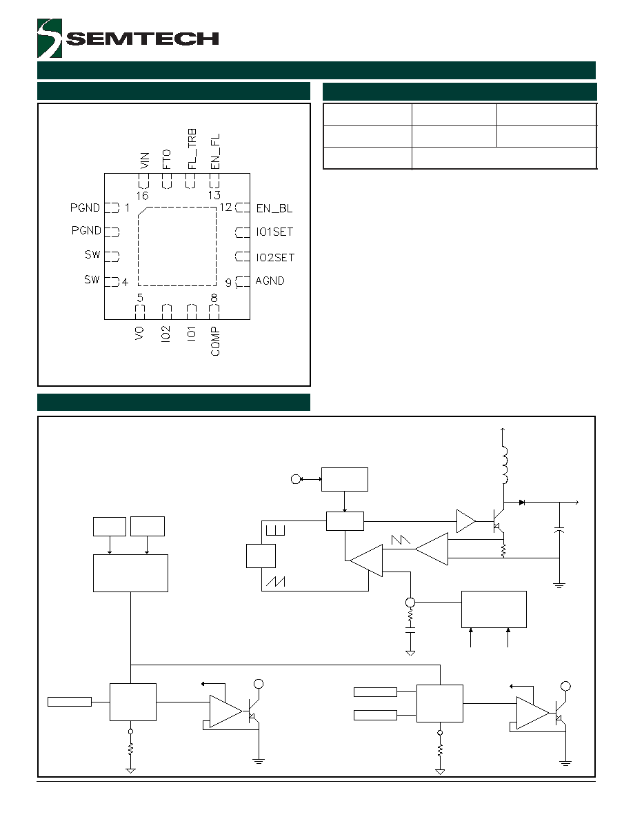
Pin Configurations
Ordering Information
TOP VIEW
(16 Pin - MLPQ)
e
c
i
v
e
D
)
2
(
)
1
(
e
g
a
k
c
a
P
T
(
e
g
n
a
R
.
p
m
e
T
A
)
T
R
T
L
M
5
0
5
4
C
S
6
1
-
Q
P
L
M
C
5
8
o
t
0
4
-
B
V
E
5
0
5
4
C
S
D
R
A
O
B
N
O
I
T
A
U
L
A
V
E
Notes:
(1) Only available in tape and reel packaging. A reel
contains 3000 devices.
(2) Lead free product. This product is fully WEEE and
RoHS compliant.
Block Diagram
EN_BL
Rsense-
5mOhm
Sense
Amp
Q
COMP
OSC
R
S
BL Setpoint
FL Setpoint
RO2SET
EN_FL
FL_TRB
Error signal selection
and summation
ADJ
1
ADJ
2
IO2SET
RO1SET
IO1SET
ADJ1
ADJ2
IO1
IO2
Reference&
Internal Regulator
UVLO
Thermal
Shutdown
VO
OVP
Comparator
VCC
VOUT
PGND
AGND
5
2006 Semtech Corp.
www.semtech.com
SC4505
POWER MANAGEMENT
Block Diagram
Pin Descriptions
n
i
P
e
m
a
N
n
i
P
n
o
i
t
c
n
u
F
n
i
P
2
,
1
D
N
G
P
.
d
n
u
o
r
g
r
e
w
o
P
4
,
3
W
S
.
e
d
o
i
d
g
n
i
y
fi
t
c
e
r
e
h
t
d
n
a
r
o
t
c
u
d
n
i
t
s
o
o
b
e
h
t
o
t
t
c
e
n
n
o
C
.r
o
t
s
i
s
n
a
r
t
r
e
w
o
p
l
a
n
r
e
t
n
i
e
h
t
f
o
r
o
t
c
e
ll
o
C
5
O
V
.
n
i
p
s
i
h
t
t
a
e
g
a
tl
o
v
e
h
t
s
r
o
ti
n
o
m
o
s
l
a
n
o
it
c
e
t
o
r
p
e
g
a
tl
o
v
r
e
v
o
l
a
n
r
e
t
n
I
.
n
i
p
e
g
a
tl
o
v
t
u
p
t
u
o
t
s
o
o
B
.
n
i
p
s
i
h
t
o
t
s
g
n
ir
t
s
D
E
L
e
h
t
f
o
e
d
o
n
a
e
h
t
d
n
a
r
o
ti
c
a
p
a
c
t
u
p
t
u
o
e
h
t
t
c
e
n
n
o
C
6
2
O
I
.
2
g
n
ir
t
s
D
E
L
o
t
t
n
e
r
r
u
c
e
c
r
u
o
s
t
n
a
t
s
n
o
c
s
e
d
i
v
o
r
P
7
1
O
I
.
1
g
n
ir
t
s
D
E
L
o
t
t
n
e
r
r
u
c
e
c
r
u
o
s
t
n
a
t
s
n
o
c
s
e
d
i
v
o
r
P
8
P
M
O
C
p
o
o
l
r
o
f
d
e
s
u
s
i
n
i
p
s
i
h
T
.r
e
if
il
p
m
a
r
o
r
r
e
e
c
n
a
t
c
u
d
n
o
c
s
n
a
r
t
l
a
n
r
e
t
n
i
e
h
t
f
o
t
u
p
t
u
o
e
h
T
.
n
o
it
a
s
n
e
p
m
o
c
9
D
N
G
A
.
d
n
u
o
r
g
g
o
l
a
n
A
0
1
T
E
S
2
O
I
e
h
t
,
D
N
G
o
t
n
i
p
s
i
h
t
m
o
r
f
d
e
t
c
e
n
n
o
c
r
o
t
s
i
s
e
r
e
h
t
g
n
it
c
e
l
e
s
y
B
.
n
i
p
t
e
s
e
u
l
a
v
2
O
I
e
c
r
u
o
s
t
n
e
r
r
u
C
.t
e
s
s
i
2
g
n
ir
t
s
n
o
t
n
e
r
r
u
c
m
u
m
i
x
a
m
g
n
i
d
n
o
p
s
e
r
r
o
c
1
1
T
E
S
1
O
I
e
h
t
,
D
N
G
o
t
n
i
p
s
i
h
t
m
o
r
f
d
e
t
c
e
n
n
o
c
r
o
t
s
i
s
e
r
e
h
t
g
n
it
c
e
l
e
s
y
B
.
n
i
p
t
e
s
e
u
l
a
v
1
O
I
e
c
r
u
o
s
t
n
e
r
r
u
C
.t
e
s
s
i
1
g
n
ir
t
s
n
o
t
n
e
r
r
u
c
m
u
m
i
x
a
m
g
n
i
d
n
o
p
s
e
r
r
o
c
2
1
L
B
_
N
E
.
)
c
i
g
o
l
r
o
f
2
e
l
b
a
T
e
e
S
(
.
1
g
n
ir
t
s
t
h
g
il
k
c
a
b
D
E
L
r
o
f
n
i
p
l
o
r
t
n
o
c
s
s
e
n
t
h
g
ir
B
d
n
a
e
l
b
a
n
E
3
1
L
F
_
N
E
.
)
c
i
g
o
l
r
o
f
1
e
l
b
a
T
e
e
S
(
.
2
g
n
ir
t
s
t
h
g
il
h
s
a
lf
D
E
L
r
o
f
n
i
p
l
o
r
t
n
o
c
s
s
e
n
t
h
g
ir
B
d
n
a
e
l
b
a
n
E
4
1
B
R
T
_
L
F
5
1
O
T
F
s
i
n
o
it
a
r
u
d
t
u
o
e
m
it
e
h
t
,
n
i
p
s
i
h
t
o
t
d
e
t
c
e
n
n
o
c
r
o
ti
c
a
p
a
c
e
h
t
g
n
it
c
e
l
e
s
y
B
.
n
i
p
t
u
o
e
m
it
h
s
a
l
F
.
d
e
l
b
a
s
i
d
s
i
n
o
it
c
n
u
f
O
T
F
e
h
t
,
D
N
G
A
o
t
n
i
p
s
i
h
t
g
n
il
l
u
p
y
B
.
d
e
n
i
m
r
e
t
e
d
6
1
N
I
V
.
n
i
p
e
h
t
o
t
e
s
o
l
c
s
r
o
ti
c
a
p
a
c
h
ti
w
d
e
s
s
a
p
y
B
.
n
i
P
y
l
p
p
u
S
r
e
w
o
P
d
a
P
d
e
s
o
p
x
E
l
a
m
r
e
h
t
d
o
o
g
r
o
f
B
C
P
e
h
t
n
o
e
n
a
l
p
d
n
u
o
r
g
g
o
l
a
n
a
e
h
t
o
t
d
e
r
e
d
l
o
s
e
b
t
s
u
m
d
a
p
d
e
s
o
p
x
e
e
h
T
.
n
o
it
c
u
d
n
o
c
Table 1
Note: When
EN_FL = 0
FL_TRB = 0
EN_BL = 0
The boost is turned OFF and disabled.
L
B
_
N
E
s
u
t
a
t
S
0
e
l
b
a
s
i
d
t
h
g
il
k
c
a
B
1
e
l
b
a
n
e
t
h
g
il
k
c
a
B
Table 2
L
F
_
N
E
B
R
T
_
L
F
s
u
t
a
t
S
0
0
e
l
b
a
s
i
d
h
s
a
l
F
0
1
e
l
b
a
s
i
d
h
s
a
l
F
1
0
y
b
t
e
s
t
n
e
r
r
u
c
t
u
p
t
u
o
.
x
a
m
%
0
2
T
E
S
2
O
R
,r
o
t
s
i
s
e
r
l
a
n
r
e
t
x
e
1
1
t
e
s
t
n
e
r
r
u
c
t
u
p
t
u
o
.
x
a
m
%
0
0
1
T
E
S
2
O
R
,r
o
t
s
i
s
e
r
l
a
n
r
e
t
x
e
y
b