 | –≠–ª–µ–∫—Ç—Ä–æ–Ω–Ω—ã–π –∫–æ–º–ø–æ–Ω–µ–Ω—Ç: SC4508 | –°–∫–∞—á–∞—Ç—å:  PDF PDF  ZIP ZIP |

POWER MANAGEMENT
1
www.semtech.com
SC4508
Buck or Buck-Boost(Inverting)
Current Mode Controller
Description
Revision: October 22, 2003
Features
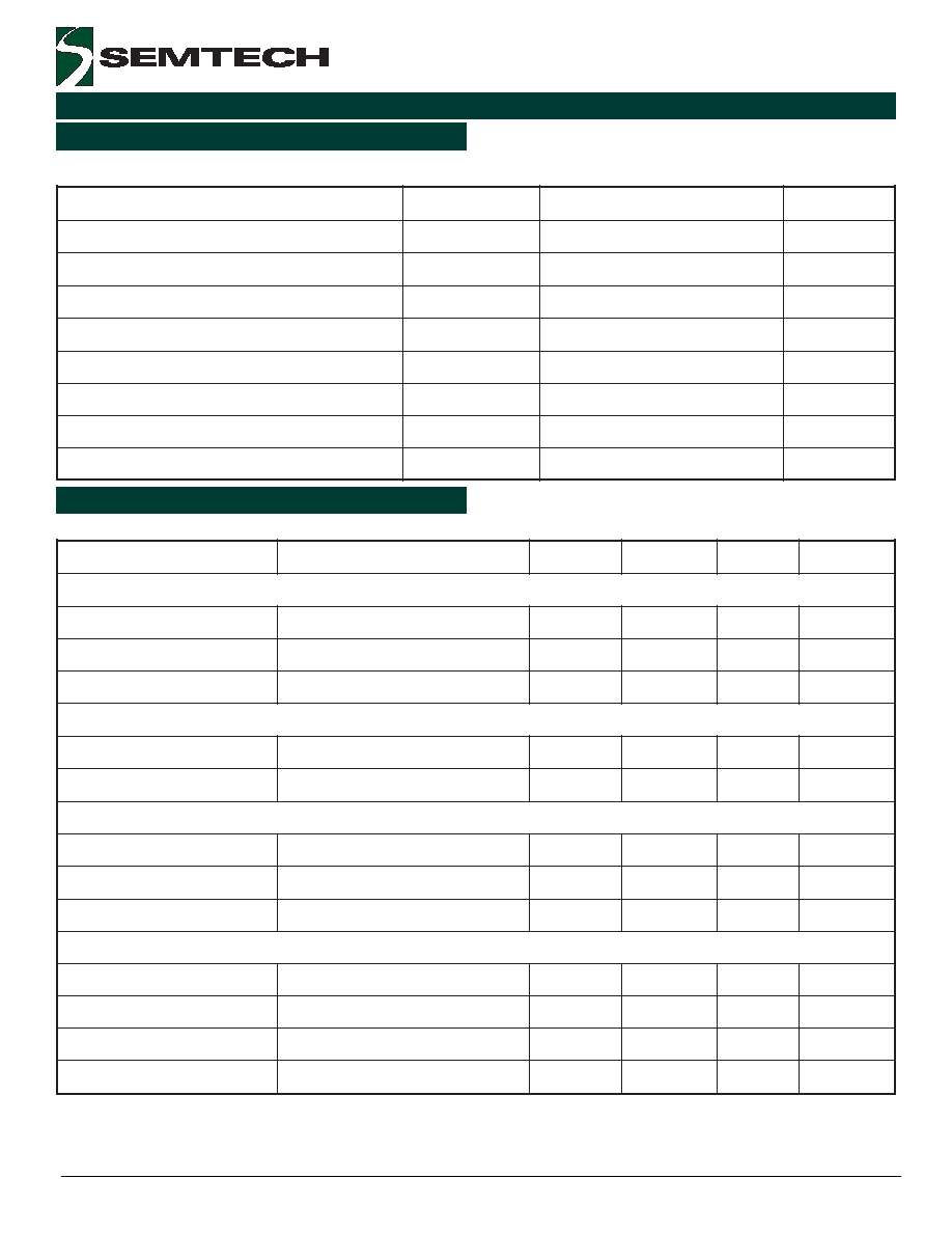
Typical Application Circuits
Applications
Wide input voltage range 2.7V to 15V
Programmable output voltage
Programmable switching frequency up to 1.5MHz
Buck or buck boost(inverting) configuration
Current mode control with slope compensation
Very low quiescent current in shutdown mode
Accessible reference voltage
Low power point of use converters
Single or multiple output low power converters
Positive and/or negative output voltage
DSL cards
Graphic cards
I/O cards
Negative bias supplies
The SC4508 is a low voltage current mode switching regu-
lator controller that drives a P-channel power MOSFET
with programmable switching frequency. It can be con-
figured in either buck or buck boost (inverting) convert-
ers. The converters can be operated from 2.7V to 15V
input voltage range. The typical operating supply current
is 3mA and a shutdown pin allows the user to turn the
controller off reducing it to less than 200
µ
A. The output
voltage can adjusted by external resistor divider. The
switching frequency is programmable up to 1.5MHz,
allowing small inductor and capacitor values to minimize
PCB space. The operating current level is programmable
via an external sense resistor. Accessible reference volt-
age allows users to make output voltage as low as they
want.
VREF
CS
OUT
VDD
FB+
FB-
COMP
SS/SHDN
OSC
SC4508
Vin
GND
CS
OSC
VDD
Vin
SS/SHDN
FB-
GND
SC4508
OUT
FB+
VREF
COMP
2
2003 Semtech Corp.
www.semtech.com
POWER MANAGEMENT
SC4508
Electrical Characteristics
Absolute Maximum Rating
Unless specified: V
DD
= 2.7V to 15V , T
A
= T
J
= -40∞C to 105∞C
r
e
t
e
m
a
r
a
P
l
o
b
m
y
S
m
u
m
i
x
a
M
s
t
i
n
U
D
N
G
o
t
D
D
V
6
1
o
t
3
.
0
-
V
D
N
G
o
t
N
D
H
S
/
S
S
2
.
3
V
D
N
G
o
t
C
S
O
,
P
M
O
C
,
-
B
F
,
+
B
F
5
V
t
n
e
r
r
u
C
F
E
R
V
1
A
m
k
n
i
S
r
o
e
c
r
u
o
S
T
U
O
0
5
2
A
m
e
g
n
a
R
e
r
u
t
a
r
e
p
m
e
T
e
g
a
r
o
t
S
T
G
T
S
0
5
1
+
o
t
0
6
-
C
∞
e
g
n
a
R
e
r
u
t
a
r
e
p
m
e
T
n
o
it
c
n
u
J
T
J
0
5
1
+
o
t
0
4
-
C
∞
.
c
e
S
0
1
)
g
n
ir
e
d
l
o
S
(
e
r
u
t
a
r
e
p
m
e
T
d
a
e
L
T
D
A
E
L
0
6
2
C
∞
r
e
t
e
m
a
r
a
P
s
n
o
i
t
i
d
n
o
C
t
s
e
T
n
i
M
p
y
T
x
a
M
t
i
n
U
y
l
p
p
u
S
r
e
w
o
P
e
g
n
a
R
e
g
a
tl
o
V
t
u
p
n
I
7
.
2
5
1
V
t
n
e
r
r
u
C
t
n
e
c
s
e
i
u
Q
w
o
l
=
N
D
H
S
0
0
2
0
0
5
A
µ
t
n
e
r
r
u
C
g
n
it
a
r
e
p
O
d
a
o
l
o
N
,
h
g
i
h
=
N
D
H
S
3
A
m
t
u
o
k
c
o
L
e
g
a
t
l
o
v
r
e
d
n
U
d
l
o
h
s
e
r
h
T
t
r
a
t
S
5
.
2
V
s
i
s
e
r
e
t
s
y
H
O
L
V
U
0
0
1
V
m
r
o
t
a
ll
i
c
s
O
e
g
n
a
R
y
c
n
e
u
q
e
r
F
0
0
1
0
0
5
1
z
H
K
y
c
n
e
u
q
e
r
F
C
T
F
p
0
0
3
=
0
5
4
0
0
5
0
5
5
z
H
K
t
n
e
r
r
u
C
e
g
r
a
h
C
0
0
1
A
µ
r
e
i
f
il
p
m
A
r
o
r
r
E
e
g
a
tl
o
V
t
u
p
n
I
k
c
a
b
d
e
e
F
5
7
.
0
V
t
n
e
r
r
u
C
s
a
i
B
t
u
p
n
I
0
0
2
A
n
e
c
n
a
t
c
u
d
n
o
c
s
n
a
r
T
5
S
m
t
n
e
r
r
u
C
k
n
i
S
r
o
e
c
r
u
o
S
t
u
p
t
u
O
0
0
1
A
µ
Exceeding the specifications below may result in permanent damage to the device, or device malfunction. Operation outside of the parameters
specified in the Electrical Characteristics section is not implied.

3
2003 Semtech Corp.
www.semtech.com
POWER MANAGEMENT
SC4508
Electrical Characteristics
r
e
t
e
m
a
r
a
P
s
n
o
i
t
i
d
n
o
C
t
s
e
T
n
i
M
p
y
T
x
a
M
t
i
n
U
r
o
t
a
r
a
p
m
o
C
M
W
P
t
u
p
t
u
O
o
t
y
a
l
e
D
0
5
s
n
e
c
n
e
r
e
f
e
R
F
E
R
V
e
g
a
tl
o
V
t
u
p
t
u
O
1
3
2
.
1
5
2
.
1
9
6
2
.
1
V
t
n
e
r
r
u
C
t
u
p
t
u
O
1
A
m
n
o
it
a
l
u
g
e
R
e
n
i
L
V
D
D
I
,
V
5
1
o
t
7
.
2
=
F
E
R
V
A
m
1
=
4
V
m
n
o
it
a
l
u
g
e
R
d
a
o
L
V
D
D
I
,
V
5
=
F
E
R
V
A
m
1
o
t
0
=
4
V
m
n
w
o
d
t
u
h
S
/
t
r
a
t
S
t
f
o
S
t
n
e
r
r
u
C
e
g
r
a
h
C
0
1
A
µ
t
n
e
r
r
u
C
e
g
r
a
h
c
s
i
D
2
1
A
m
e
g
a
tl
o
V
t
h
g
i
H
c
i
g
o
L
N
D
H
S
2
V
e
g
a
tl
o
V
w
o
L
c
i
g
o
L
N
D
H
S
5
2
.
0
V
t
i
m
i
L
t
n
e
r
r
u
C
d
l
o
h
s
e
r
h
T
e
l
c
y
C
y
b
e
l
c
y
C
2
1
.
0
V
d
l
o
h
s
e
r
h
T
n
w
o
d
t
u
h
S
6
1
.
0
V
t
u
p
t
u
O
o
t
y
a
l
e
D
0
5
S
n
t
u
p
t
u
O
)
H
(
e
c
n
a
t
s
i
s
e
R
-
n
O
e
v
ir
D
e
t
a
G
V
D
D
I
,
V
5
=
G
N
I
C
R
U
O
S
A
m
0
5
2
=
0
2
m
h
O
)
L
(
e
c
n
a
t
s
i
s
e
R
-
n
O
e
v
ir
D
e
t
a
G
V
D
D
I
,
V
5
=
K
N
I
S
A
m
0
5
2
=
0
2
m
h
O
e
m
i
T
e
s
i
R
C
T
U
O
F
p
0
0
2
=
0
2
S
n
e
m
i
T
ll
a
F
C
T
U
O
F
p
0
0
2
=
0
2
S
n
Unless specified: V
DD
= 2.7V to 15V , T
A
= T
J
= -40∞C to 105∞C
Note:
(1) This device is ESD sensitive. Use of standard ESD handling precautions is required.

4
2003 Semtech Corp.
www.semtech.com
POWER MANAGEMENT
SC4508
#
n
i
P
e
m
a
N
n
i
P
n
o
i
t
c
n
u
F
n
i
P
1
T
U
O
.t
u
p
t
u
o
e
v
ir
d
e
t
a
G
2
S
C
.
e
s
n
e
s
ti
m
il
t
n
e
r
r
u
C
3
N
D
H
S
/
S
S
.
e
c
i
v
e
d
e
h
t
n
w
o
d
t
u
h
s
o
t
w
o
l
d
l
o
H
.
n
i
p
t
r
a
t
s
tf
o
S
4
F
E
R
V
.t
u
p
t
u
o
e
g
a
tl
o
v
e
c
n
e
r
e
f
e
r
V
5
2
.
1
5
C
N
.
n
o
it
c
e
n
n
o
c
o
N
6
D
N
G
A
.
d
n
u
o
r
g
g
o
l
a
n
A
7
D
N
G
P
.
d
n
u
o
r
g
r
e
w
o
P
8
-
B
F
.t
u
p
n
i
g
n
it
r
e
v
n
i
r
e
if
il
p
m
a
r
o
r
r
E
9
+
B
F
.t
u
p
n
i
g
n
it
r
e
v
n
i-
n
o
n
r
e
if
il
p
m
a
r
o
r
r
E
0
1
P
M
O
C
.
n
o
it
a
s
n
e
p
m
o
c
r
o
f
t
u
p
t
u
o
r
e
if
il
p
m
a
r
o
r
r
E
1
1
C
S
O
.
y
c
n
e
u
q
e
r
f
r
o
t
a
ll
i
c
s
o
m
m
a
r
g
o
r
p
o
t
D
N
G
o
t
r
o
ti
c
a
p
a
c
a
t
c
e
n
n
o
C
2
1
D
D
V
.
e
g
a
t
o
v
y
l
p
p
u
S
Pin Descriptions
Notes:
(1) Only available in tape and reel packaging. A reel
contains 3000 devices.
(2) Lead free product.
E
C
I
V
E
D
)
1
(
E
G
A
K
C
A
P
T
(
e
g
n
a
R
.
p
m
e
T
J
)
R
T
L
M
I
8
0
5
4
C
S
2
1
-
P
L
M
C
∞
0
5
1
o
t
C
∞
0
4
-
T
R
T
L
M
I
8
0
5
4
C
S
)
2
(
Ordering Information
Pin Configuration
TOP VIEW
(MLP12 4x4)
1
OUT
2
CS
3
SS/SHDN
9
FB+
8
FB-
7
PGND
4
VREF
5
NC
6
AGND
12
VDD
11
10
OSC
COMP

5
2003 Semtech Corp.
www.semtech.com
POWER MANAGEMENT
SC4508
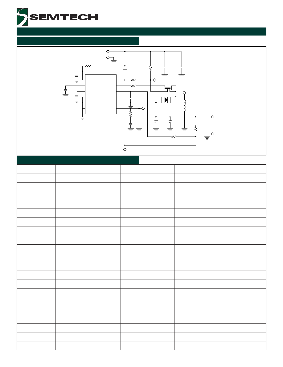
Block Diagram
Marking Information
Top View
yyww = Date Code (Example: 0012)

6
2003 Semtech Corp.
www.semtech.com
POWER MANAGEMENT
SC4508
Application Information
The SC4508 is designed to control buck (step down) or
buck-boost (inverting) converter with P-channel MOSFET
as a switch using current mode, programmable switching
frequency architecture. During steady state operation,
the switch is turned on each cycle and turned off when
the voltage across current sense resistor exceeds the
voltage level at COMP pin set by voltage loop error
amplifier. A fixed 0.5V artificial ramp is added internally
to the sensed current signal for operations when duty-
cycle is larger than 50%. In over load or output shortage
condition, if the sensed current signal reaching typical
120mV, the switch is turned off immediately in the same
cycle. If the sensed current signal further increases to
typical 160mV, not only the switch is turned off but also
the soft start capacitor is discharged by a internal MOSFET
to ground then charging back to threshold 250mV during
which the switch is held off. With the "hiccup" mode over
current protection, the thermal stress is reduced in the
faulty conditions.
Current Sense and Current Limit
The typical cycle-by-cycle current limit threshold in the
current sense pin of the SC4508 is 120mV. The over
current limit is assumed typical 120% of full load current.
Then the current sense resistor can be calculated by the
following equation:
Rs =
)
pk
(
I
%
120
mV
120
L
∑
I
L
(pk) =
)
V
V
V
V
(
L
f
V
V
2
1
I
D
IN
D
O
s
O
IN
O
+
+
∑
-
+
for Buck
Boost
Buck
for
)
V
V
V
V
V
(
L
f
V
2
1
V
V
V
V
I
)
pk
(
I
D
O
IN
D
O
s
IN
IN
D
O
IN
O
L
-
+
+
+
∑
+
+
+
=
I
O
- full load current
V
O
- output voltage
V
IN
- input voltage
V
D
- diode forward voltage drop
f
S
- switching frequency
L - inductor
Inductor Selection
A inductor is chosen based on the required output ripple
current which is usually 20-30% of load current. The ripple
current
I decreases with higher inductance and
increases with higher input voltage V
IN
or output voltage
V
O.
)
V
V
V
V
(
I
f
V
V
L
D
IN
D
O
L
s
O
IN
+
+
∑
-
=
for Buck
)
V
V
V
V
V
(
I
f
V
L
D
O
IN
D
O
L
s
IN
+
+
+
∑
=
for Buck-Boost
Specify the maximum inductor current larger than I
L
(pk)
set by the current sense resistor R
S
to avoid the inductor
core saturation.
Input Capacitor C
IN
and Output Capacitor C
OUT
Selection
Both input and output capacitors need to be sized to
handle the ripple current safely. Buck converters have
high ripple current in the input side while buck-boost
converters have high ripple current in the both input and
output capacitors. Therefore, the RMS value of the
current must be less than the high frequency ripple rating
of the capacitors. In continuous mode operation,
IN
O
IN
O
O
CAP
_
INPUT
_
RMS
V
)
V
V
(
V
I
I
-
for Buck
IN
D
O
O
CAP
_
RMS
V
V
V
I
I
+
for Buck-Boost input and output
capacitors.
The C
OUT
is selected for Buck converter is by required
output ripple voltage and converter loop stability. The
output ripple is determined by:
)
C
f
8
1
ESR
(
I
V
OUT
s
L
O
+
where f
S
is converted switching frequency, C
OUT
is output
capacitance and
I
L
is inductor ripple current.

7
2003 Semtech Corp.
www.semtech.com
POWER MANAGEMENT
SC4508
Application Information (Cont.)
In Buck converter, the worst case input RMS ripple current
occurs at 50% duty cycle, or at V
IN
= 2V
OUT
. Under this
condition, the input capacitors RMS ripple current is about
half of the load current.
MOSFET Selection
The selection criteria for the power MOSFET is its
operating junction temperature not exceeding the
maximum junction temperature. Therefore, from a
specified ambient temperature, the maximum junction
to ambient temperature rise has to be determined, which
is related to the MOSFET power dissipation or power loss.
The power loss includes conduction loss and switching
loss. The conduction loss is given by:
)
ON
(
DS
2
O
D
IN
D
O
ON
R
I)
V
V
V
V
(
P
+
+
=
for Buck
)
ON
(
DS
2
O
D
O
IN
D
O
IN
ON
R
I)
V
V
)(
V
V
V
V
(
P
+
+
+
=
for Buck-Boost
Freewheeling Diode Selection
The Schottky diode is recommended as freewheeling
diode in the both Buck and Buck-Boost applications. The
diode conducts during the off-time. The diode voltage
and current ratings are selected based upon the peak
reverse voltage, the peak current and average power
dissipation.
Buck
for
V
V
V
V
I
I
,
2
I
I
I
,
V
V
D
IN
O
IN
O
)
AVG
(
D
L
O
)
PEAK
(
D
IN
)
REV
(
D
+
-
=
+
=
=
Boost
Buck
for
I
I,
2
I
)
V
V
V
V
(
I
I
,
V
V
V
O
)
AVG
(
D
L
IN
D
O
IN
O
)
PEAK
(
D
O
IN
)
REV
(
D
-
=
+
+
+
=
+
=
The most stressful condition for the diode occurs when
the output is shorted. Under this condition, due to the
V
OUT
= 0, the diode conducts at close to 100% duty cycle.
Therefore, attention should be paid to the thermal
condition when laying out a board.
LAYOUT GUIDELINES
Careful attention to layout requirements are necessary
for successful implementation of the SC4508 PWM con-
troller. High switching currents are present in the appli-
cation and their effect on ground plane voltage differen-
tials must be understood and minimized.
1). The high power parts of the circuit should be laid out
first. A ground plane should be used, the number and
position of ground plane interruptions should be such as
to not unnecessarily compromise ground plane integrity.
Isolated or semi-isolated areas of the ground plane may
be deliberately introduced to constrain ground currents
to particular areas, for example, the input capacitor and
output capacitor ground.
2). The loop formed by the Input Capacitor(s) (Cin), the
MOSFET and the Schottky diode or inductor must be kept
as small as possible. This loop contains all the high cur-
rent, fast transition switching. Connections should be as
wide and as short as possible to minimize loop induc-
tance
3). The connection between the junction of MOSFET,
Schottky diode and the output inductor should be a wide
trace or copper region. It should be as short as practical.
Since this connection has fast voltage transitions, keep-
ing this connection short will minimize EMI.
4) The Output Capacitor(s) (Cout) should be located as
close to the load as possible, fast transient load cur-
rents are supplied by Cout only, and connections between
Cout and the load must be short, wide copper areas to
minimize inductance and resistance.
5) A separate analog ground plane connects to the
SC4508 AGND pin. All analog grounding path including
decoupling capacitors, feedback resistors, compensation
components, and current-limit setting resistors should
be connected to this plane.

8
2003 Semtech Corp.
www.semtech.com
POWER MANAGEMENT
SC4508
Evaluation Board Schematic, Buck
12V
TP1
GND
TP2
f s=1.08MHz
R2 10
C4
0.1uF
R3 2.2
C3
1nF
C6
68pF
U2 FDFS2P102A
1
2
3
4
5
6
7
8
C1
47uF/16V
C10
2nF
R4
20K
C7
0.1uF
L1
3.3uH
C2
47uF/16V
TP4
R6
NOT POPULATED
TP5
1.25V/2A
SC4508
U1
10
5
3
11
9
8
4
1
2
12
6
7
COMP
NC
SS/SHDN
OSC
FB+
FB-
VREF
OUT
CS
VDD
AGND
PGND
C9
680uF/4V
GND
R5
750
C11
2.7nF
TP3
R1
0.015
C8
680uF/4V
R7 10
C5
0.1uF
Bill of Materials
m
e
t
I
y
t
i
t
n
a
u
Q
e
c
n
e
r
e
f
e
R
t
r
a
P
r
e
r
u
t
c
a
f
u
n
a
M
1
2
2
C
,
1
C
V
6
1
/
F
u
7
4
M
7
4
B
P
T
6
1
:
N
/
P
o
y
n
a
S
2
1
3
C
F
n
1
3
3
7
C
,
5
C
,
4
C
F
u
1
.
0
4
1
6
C
F
p
8
6
5
2
9
C
,
8
C
V
4
/
F
u
0
8
6
6
1
0
1
C
F
n
2
8
1
1
O
J
A
2
/
V
5
2
.
1
9
1
3
O
J
V
2
1
0
1
2
3
D
N
G
1
O
J
,
1
D
N
G
1
O
J
D
N
G
1
1
1
1
L
H
u
3
.
3
2
1
1
1
R
5
1
0
.
0
3
1
2
7
R
,
2
R
0
1
4
1
1
3
R
2
.
2
5
1
1
4
R
K
0
2
6
1
1
5
R
0
5
7
7
1
1
6
R
d
e
t
a
l
u
p
o
p
t
o
n
8
1
8
8
P
T
-
1
P
T
R
T
N
I
O
P
T
9
1
1
1
U
8
0
5
4
C
S
.
p
r
o
C
h
c
e
t
m
e
S
0
2
1
2
U
A
2
0
1
P
2
S
F
D
F
:
N
/
P
d
li
h
c
r
i
a
F
A
2
0
1
P
2
S
F
D
F
9
2003 Semtech Corp.
www.semtech.com
POWER MANAGEMENT
SC4508
Evaluation Board Schematic, Buck-Boost
C11
2.7nF
C1
47uF/16V
C8
47uF/16V
R1
0.015
GND
C3
1nF
C4
0.1uF
R3 2.2
C2
47uF/16V
R7 10
TP3
R6 1.24K
TP4
C7
0.1uF
GND
C6
300pF
C10
100pF
C5
0.1uF
SC4508
U1
10
5
3
11
9
8
4
1
2
12
6
7
COMP
NC
SS/SHDN
OSC
FB+
FB-
VREF
OUT
CS
VDD
AGND
PGND
R2 100
C9
47uF/16V
12V
R4
20K
R5
10K
TP1
TP5
-10V/1A
U2 FDFS2P102A
1
2
3
4
5
6
7
8
L1
3.3uH
m
e
t
I
y
t
i
t
n
a
u
Q
e
c
n
e
r
e
f
e
R
t
r
a
P
r
e
r
u
t
c
a
f
u
n
a
M
1
4
9
C
,
8
C
,
2
C
,
1
C
V
6
1
/
F
u
7
4
M
7
4
B
P
T
6
1
:
N
/
P
o
y
n
a
S
2
1
3
C
F
n
1
3
3
7
C
,
5
C
,
4
C
F
u
1
.
0
4
1
6
C
F
p
0
0
3
5
1
0
1
C
F
p
0
0
1
6
1
1
1
C
F
n
7
.
2
7
1
1
O
J
A
1
/
V
0
1
-
8
1
3
O
J
V
2
1
9
2
3
D
N
G
1
O
J
,
1
D
N
G
1
O
J
D
N
G
0
1
1
1
L
H
u
3
.
3
1
1
1
1
R
5
1
0
.
0
2
1
1
2
R
0
0
1
3
1
1
3
R
2
.
2
4
1
1
4
R
K
0
2
5
1
1
5
R
K
0
1
6
1
1
6
R
K
4
2
.
1
7
1
7
R
0
1
8
1
8
8
P
T
-
1
P
T
R
T
N
I
O
P
T
9
1
1
1
U
8
0
5
4
C
S
.
p
r
o
C
h
c
e
t
m
e
S
0
2
1
2
U
A
2
0
1
P
2
S
F
D
F
:
N
/
P
d
li
h
c
r
i
a
F
A
2
0
1
P
2
S
F
D
F
Bill of Materials

10
2003 Semtech Corp.
www.semtech.com
POWER MANAGEMENT
SC4508
Contact Information
Semtech Corporation
Power Management Products Division
200 Flynn Road, Camarillo, CA 93012
Phone: (805)498-2111 FAX (805)498-3804
Outline Drawing - MLP-12